Continue to Site

Welcome to EDAboard.com

Welcome to our site! EDAboard.com is an international Electronics Discussion Forum focused on EDA software, circuits, schematics, books, theory, papers, asic, pld, 8051, DSP, Network, RF, Analog Design, PCB, Service Manuals... and a whole lot more! To participate you need to register. Registration is free. Click here to register now.

Reactance modulation...

Status
Not open for further replies.

aj_silverthunder

Full Member level 3
Joined
Jul 30, 2009
Messages
179
Helped
0
Reputation
0
Reaction score
0
Trophy points
1,296
Location
asia
Activity points
2,601
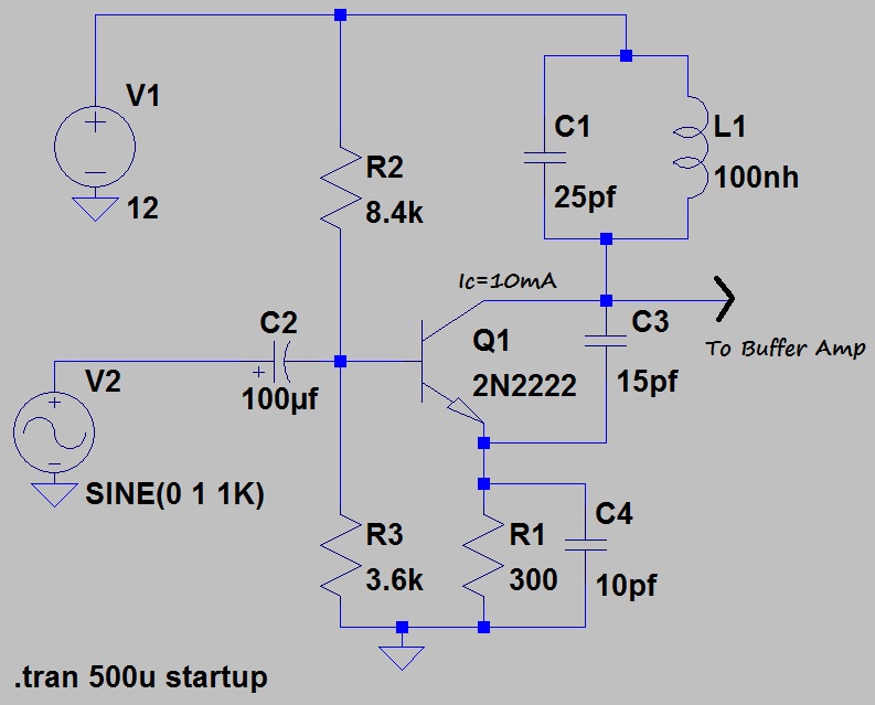
guys in tthe schematic its a reactance modulation,my confusion is about the output signal from the oscillator,
guys from wich point can i take the output signal from the tank circuit to the next buffer amp stage...in the
schematic,do u think the output can be taken out from under the inductor to the next buffer amp stage,please
help me,its very crucial thing for me now,thank u
i think the output must be from the collector of the transistor,am i right or wrong,if wrong,please correct me,


Added after 24 minutes:


Hi aj,

You could take the ouput at the collector or at the emitter:
You have a high-impedance output at the collector and a low-impedance output at the emitter (with lower voltage level and higher current capability).
At the collector, the circuit is more sensitive to the effect of the load (the following stage): the load reactance can affect the frequency and the resistence could avoid oscillation.
It is safer to take the output at the emitter.
Regards

Z
 

Hello,

I think when you are going to build this circuit, you need a capacitor between the base and ground. I assume this is a common base oscillator.

Now for AC the base is grounded via V2, but in reality this may be a non-low impedance source at the oscillation frequency.

You can check this by removing C2 and V2 and see whether it still oscillates.
 

Hello,

Very strange as you have a capacitor between C and E and the base is grounded via C2 and V2 (for RF). Your emitter is also not grounded for RF

What is your RF base voltage during oscillation (make V2 zero, so there is no modulation)?
 

I agree with WimRFP.
C4 is too small (comare with C1 and C3) for a decoupling capacitor.
This circuit has the structure of an oscillator. It doesn't look like a reactance modulator. Are you sure it is? Is it intended to oscillate?
Have you a more complete schematic?
Regards

Z
 

do u think this is better ,its a colpitt oscillator,modulated by varactor,please check it
 

Hello,

If linearity is not that importance, you can change the bias point (base voltage) with the LF signal to get frequency modulation. You will also get some AM, but that will disappear (probably) because of clipping of subsequent stages.

I expected that the other circuit also was an oscillator where you make FM by varying the base voltage (via the 100uF capacitor).

Other option is to use 1 or 2 varactor diodes (variable capacitance diodes).
 

yes u got me correct on the previous schematic...it was a reactance modulation,but i think in practical,its of no use..because it becomes a Tunned collector amplifer...and has some disadvantages like..the voltage swing at the collector goes very higher ...and it has no feed back,so the oscillations will dampen....
do u think i am right

Added after 4 minutes:

and in this new one its a colpitt,modulated by varactor......and the varactor is isolated by the capacitor C9..do u think it works..


Hello,

If you make sure that the RF voltage across the varactor will not forward bias the diode, this may work. But.... don't forget to add a choke (or resistor) between the varactor and C8, as you almost short circuit the varactor with C8 and V3.

I didn't check the oscillator, but you will probably verify with simulation. You have to experiment with C4 to get best oscillation, making it too large or too small may kill your oscillation. My feeling says that you have to increase C12.
 

OK, now it is an oscillator modulated with a varactor.
There was a misunderstanding because a "reactance modulator" is a different device, that achieves variable reactance modulating the transconductance of a transistor.
I would adopt a more clear Colpitts topology; for instance, I don't like the lack of a capacitor between C and E. I don't say that this circuit does not oscillate as is in the schematic, but it can do so because of parassitic elements. In this case, frequency stability could be poor.
Regards

Z
 

guys please tell me is there any shorting in the oscillator,i have added a resistor to avoid shorting from C8 capacitor...
and do u think the audio source can short the varactor..
and do think the two caps C3(12pF) and C5(12pF) forms a series capacitance so its value will be 6pF....
 

Hello,

Adding the resistor is OK, the audio source will not short your varactor.

Basically you are right, they form a series circuit. But C5 is in parallel with the base bias resistors and the input of the transistor with emitter resistor/capacitance, so the effective capacitance will be less then 6 pF in this case.

You should increase C5 to get a better match to the input impedance of the amplifier. the Q factor of the LC circuit will drop to a very low value now.

I think you also must increase C4 somewhat to get more gain from the amplifier. Try this with simulation. don't make it to be a short circuit, as some capacitive effect in the emitter helps these circuits to oscillate better.

I expect this circuit to be not very stable as the temperature dependent parasitics of the transistor (BE capacitance, CB capacitance) are not small with respect to your resonating capacitors.
 

Status
Not open for further replies.

Similar threads

Part and Inventory Search

Welcome to EDABoard.com

Sponsor

Back
Top