Continue to Site

Welcome to EDAboard.com

Welcome to our site! EDAboard.com is an international Electronics Discussion Forum focused on EDA software, circuits, schematics, books, theory, papers, asic, pld, 8051, DSP, Network, RF, Analog Design, PCB, Service Manuals... and a whole lot more! To participate you need to register. Registration is free. Click here to register now.

same net drc in Altium Designer

Status
Not open for further replies.

Valere Versnip

Newbie level 4
Joined
Jul 31, 2009
Messages
5
Helped
0
Reputation
0
Reaction score
0
Trophy points
1,281
Activity points
1,332
Hello,

I'm wondering quite some time now if it is possible to check for same net clearances in altium designer?

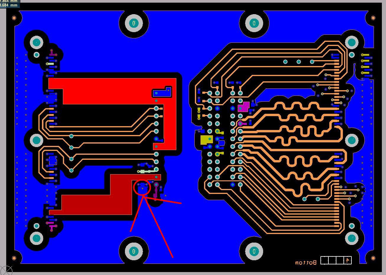
I often place groundfills on top and bottom (along with the routing). I give these polygons a big clearance, so they do not interfere with the controlled impedance of traces. Example --> see screenshot.


But: when I do this there are random places where the clearance between the groundfill polygon, and other same net objects are too small for manufacturing. Look at this screenshot (red oval is zoom in of previous screenshot):


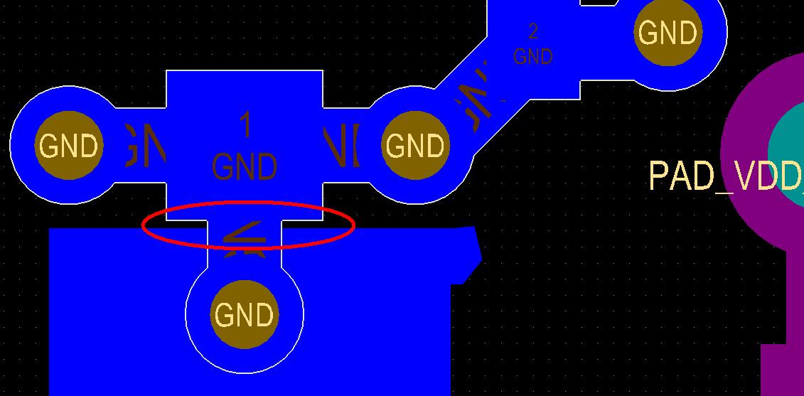
So the big thing here is: if the pad touches the polygon (so if it is connected), there should not be an error. But if the pad doesn't touch the polygon, I should be able to create an error if the clearance is smaller than the default clearance.
I have tried with the queries, but I cannot get it right.

Difficult explanation for somthing simple :D

Any suggestions?

PS: I also use Allegro, and this has a same net drc that creates errors when this happens...

Thx
 

in the design rules you can set this
"ispad" to "inpoly" and set the scope to same net only
 

Yes, I know,

But then altium reports also all the pads that are touching or inside the polygon of the same net. This aren't errors.

So it's only pads that just missed the polygon. There is a really small "air gap" between these pads and the polygon.These things give manufacture problems.

So, just using the "same net only" option, isn't an option.
 

I ran in to a similar issue just a few days ago as a novice Altium user.

The problem is that the clearance rules, by default, only apply to different net objects.

You can set the polygon pour style to not overlap same net objects. However, the gui text is deceptive, as it will avoid lines, arcs, etc. but it will still try to connect to pads and vias. You see this clearly in your second picture. The reason the pour hasn't completely overwhelmed the pad is the line elements thru the pad are keeping it back some based on the line-to-line clearance rule!

The solution is to create a polygon plane connection rule, which makes that polygon be a "No Connect" rather than "Direct" or "Thermal". This will get rid of your problem. If you have other pours on the top/bot layer you can give your pour a name "groundfill" and make the rule use IsNamedPolygon("groundfill") so the rule affects only it.

Be careful, the clearance rules use InPoly[gon] or InNamedPolygon() whereas the connection rules use IsPoly[gon] or IsNamedPolygon(). And Altium will only give you a warning/error in one of the four miss-use cases, all others it fails silently. (This is because the clearance rule is actually being applied to the primitives in the polygon.)

Also, when making the connection rule, the partner to the polygon can be "All", or "IsPad" (if you don't mind it touching the vias), etc. You can even make the pour style not avoid the same-net line elements if you prefer.

Added after 8 minutes:

Re reading your post and first response more carefully, you can probably just set the pour style property to cover all same-net objects instead of only same-net polygons, which may be the default. Then it should pour over everything.

I'd recommend against this, as it will create soldering hazards as your GND pads will effectively have more volume than the other pin(s) of the parts. Or set the connection style/rule to be 90-degree thermals while allowing the polygon to pour over all same-net polygons.

A pad surrounded by solid (non thermal) copper is effectively (2 × solder-mask-swell) larger than its partner(s) that only have a thin trace running to them. Can sometimes cause tombstoning due to unequal surface tension of liquid solder.
 

Hello,

It seems not to be clear yet :D

I don't mind that the pads or vias are a direct connect with the groundfill on top.

I WANT all the groundpads and vias to be a direct connect to the groundfill.

But I also want a clearance of 50 mils to all other different net objects. (not to influence impedances etc.)

So in the pcb I have set up a clearance rule for this pcb:
This polygon against all different nets to be 50mils. The polygon is set to: pour over all same net objects (which is what I want by the way)

But by doing this, I get "slivers" in random spots of the pcb, where a different net object "pushes" my polygon 50 mils away. But because same net clearances aren't checked, there are places where the clearance is too small as in the picture.
If I turn on same net clearances, altium will check for all the same net objects, and create unwanted errors.

So what I want:

If a ground-pad, via, track,etc TOUCHES or is IN the groundpolygon --> OK for me and no error should be produced

If a ground-pad,via,track, etc is very very close to the polygon (less than the minimum copper clearance for example: 5mils) --> will give manufacture problems, not ok for me, and an error should be produced.

I know, it is a very confusing explanation, but I don't know how to do it better
:D

Thx
 

Ok, read more more closely. :D This isn't a pad vs line backof for same net, you are correct, it is the fact that your GND pad edge is just at ~45away from your other net, which leaves a small 50-45 == 5 mil sliver since the pour backs away 50 mil.

Not sure Altium has a rule that will show up as a DRC (typically pours are calculated such that they violate no rules. rather than generating DRCs after the fact. And there may not be a rule for what you want. in which direction would you have the tool avoid the fab hazzard? By filling in or backing off?)

1. Ignore it and see/ask what the fab house says. Usually small features like this are considered problematic because they may not etch all the way. But since it is same-net you don't care if the GND plane connects a bit more to the GND pad than is shown in the artwork.

2. Manually place cut-outs in the problematic locations to avoid slivers. GND pads already have sufficient lines/vias to GND plane.

3. Create a "local" GND pour near these parts with a smaller clearance rule to fill in the slivers.

4. Avoid the problem by moving the cap south 5 mil. :p
 

Hello again,

I'm glad we are on the same subject now :D

I would like the polygon pour to back off the minimum clearance of the groundpad.

For now, I am going to ask the fabhouse what their solution is.
manually fix these things isn't an option because this happens at a lot of random places. The pcb in the screenshot is not a complex one, but some of my boards have more than 3000 components, and I don't see me manually searching all the errors :D

But for these boards I use allegro anyway.

Thx for the help!
 

Status
Not open for further replies.

Part and Inventory Search

Welcome to EDABoard.com

Sponsor

Back
Top