Herc11
Newbie level 5
Hi all,
I have downloaded a model file for tsmc018 and I’ve created two capture parts, one for the NMOS and one for the PMOS. I’ve designed two very simple circuits to test if they work. Although, the NMOS works, PMOS does not. More particularly, the result of the simulation is :
**** INCLUDING 12-SCHEMATIC1.net ****
* source 12
V_V1 N00029 0 DC 0
M_Q4 0 N00029 0 CMOSP
----------------------------------------$
ERROR -- Missing model
**** RESUMING 12-SCHEMATIC1-2.sim.cir ****
.END
I provide the definition of the model :
.MODEL CMOSP PMOS ( LEVEL = 7
+VERSION = 3.1 TNOM = 27 TOX = 4.2E-9
+XJ = 1E-7 NCH = 4.1589E17 VTH0 = -0.4349298
+K1 = 0.6076257 K2 = 0.0240727 K3 = 0
+K3B = 10.1162091 W0 = 1E-6 NLX = 8.008684E-8
+DVT0W = 0 DVT1W = 0 DVT2W = 0
+DVT0 = 0.4263447 DVT1 = 0.2825945 DVT2 = 0.1
+U0 = 118.2923681 UA = 1.595982E-9 UB = 1.109698E-21
+UC = -1E-10 VSAT = 1.682653E5 A0 = 1.6728458
+AGS = 0.4152711 B0 = 1.855408E-6 B1 = 5E-6
+KETA = 0.0180992 A1 = 0.5086627 A2 = 0.3747271
+RDSW = 296.9038493 PRWG = 0.5 PRWB = -0.3874288
+WR = 1 WINT = 0 LINT = 1.914706E-8
+XL = -2E-8 XW = -1E-8 DWG = -2.400357E-8
+DWB = 1.079858E-8 VOFF = -0.097118 NFACTOR = 1.8520072
+CIT = 0 CDSC = 2.4E-4 CDSCD = 0
+CDSCB = 0 ETA0 = 0.0163774 ETAB = -0.1095661
+DSUB = 0.7737497 PCLM = 2.3031926 PDIBLC1 = 1.921807E-4
+PDIBLC2 = 0.0174673 PDIBLCB = -9.975699E-4 DROUT = 0
+PSCBE1 = 2.054597E9 PSCBE2 = 5.934159E-10 PVAG = 15
+DELTA = 0.01 RSH = 7.5 MOBMOD = 1
+PRT = 0 UTE = -1.5 KT1 = -0.11
+KT1L = 0 KT2 = 0.022 UA1 = 4.31E-9
+UB1 = -7.61E-18 UC1 = -5.6E-11 AT = 3.3E4
+WL = 0 WLN = 1 WW = 0
+WWN = 1 WWL = 0 LL = 0
+LLN = 1 LW = 0 LWN = 1
+LWL = 0 CAPMOD = 2 XPART = 0.5
+CGDO = 6.74E-10 CGSO = 6.74E-10 CGBO = 1E-12
+CJ = 1.124859E-3 PB = 0.8637387 MJ = 0.4237235
+CJSW = 1.889062E-10 PBSW = 0.6187797 MJSW = 0.2845939
+CJSWG = 4.22E-10 PBSWG = 0.6187797 MJSWG = 0.2845939
+CF = 0 PVTH0 = 1.8347E-3 PRDSW = 15.2709708
+PK2 = 2.005769E-3 WKETA = 2.478814E-3 LKETA = 1.457236E-3
+PU0 = -2.0661953 PUA = -8.44317E-11 PUB = 1E-21
+PVSAT = -5.8202946 PETA0 = 1E-4 PKETA = 2.75599E-3 )
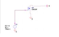
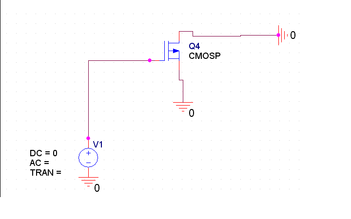
and the design of the circuit is:
Any ideas for why it does not work?
Thank you in advance,
Herc11
I have downloaded a model file for tsmc018 and I’ve created two capture parts, one for the NMOS and one for the PMOS. I’ve designed two very simple circuits to test if they work. Although, the NMOS works, PMOS does not. More particularly, the result of the simulation is :
**** INCLUDING 12-SCHEMATIC1.net ****
* source 12
V_V1 N00029 0 DC 0
M_Q4 0 N00029 0 CMOSP
----------------------------------------$
ERROR -- Missing model
**** RESUMING 12-SCHEMATIC1-2.sim.cir ****
.END
I provide the definition of the model :
.MODEL CMOSP PMOS ( LEVEL = 7
+VERSION = 3.1 TNOM = 27 TOX = 4.2E-9
+XJ = 1E-7 NCH = 4.1589E17 VTH0 = -0.4349298
+K1 = 0.6076257 K2 = 0.0240727 K3 = 0
+K3B = 10.1162091 W0 = 1E-6 NLX = 8.008684E-8
+DVT0W = 0 DVT1W = 0 DVT2W = 0
+DVT0 = 0.4263447 DVT1 = 0.2825945 DVT2 = 0.1
+U0 = 118.2923681 UA = 1.595982E-9 UB = 1.109698E-21
+UC = -1E-10 VSAT = 1.682653E5 A0 = 1.6728458
+AGS = 0.4152711 B0 = 1.855408E-6 B1 = 5E-6
+KETA = 0.0180992 A1 = 0.5086627 A2 = 0.3747271
+RDSW = 296.9038493 PRWG = 0.5 PRWB = -0.3874288
+WR = 1 WINT = 0 LINT = 1.914706E-8
+XL = -2E-8 XW = -1E-8 DWG = -2.400357E-8
+DWB = 1.079858E-8 VOFF = -0.097118 NFACTOR = 1.8520072
+CIT = 0 CDSC = 2.4E-4 CDSCD = 0
+CDSCB = 0 ETA0 = 0.0163774 ETAB = -0.1095661
+DSUB = 0.7737497 PCLM = 2.3031926 PDIBLC1 = 1.921807E-4
+PDIBLC2 = 0.0174673 PDIBLCB = -9.975699E-4 DROUT = 0
+PSCBE1 = 2.054597E9 PSCBE2 = 5.934159E-10 PVAG = 15
+DELTA = 0.01 RSH = 7.5 MOBMOD = 1
+PRT = 0 UTE = -1.5 KT1 = -0.11
+KT1L = 0 KT2 = 0.022 UA1 = 4.31E-9
+UB1 = -7.61E-18 UC1 = -5.6E-11 AT = 3.3E4
+WL = 0 WLN = 1 WW = 0
+WWN = 1 WWL = 0 LL = 0
+LLN = 1 LW = 0 LWN = 1
+LWL = 0 CAPMOD = 2 XPART = 0.5
+CGDO = 6.74E-10 CGSO = 6.74E-10 CGBO = 1E-12
+CJ = 1.124859E-3 PB = 0.8637387 MJ = 0.4237235
+CJSW = 1.889062E-10 PBSW = 0.6187797 MJSW = 0.2845939
+CJSWG = 4.22E-10 PBSWG = 0.6187797 MJSWG = 0.2845939
+CF = 0 PVTH0 = 1.8347E-3 PRDSW = 15.2709708
+PK2 = 2.005769E-3 WKETA = 2.478814E-3 LKETA = 1.457236E-3
+PU0 = -2.0661953 PUA = -8.44317E-11 PUB = 1E-21
+PVSAT = -5.8202946 PETA0 = 1E-4 PKETA = 2.75599E-3 )
and the design of the circuit is:
Any ideas for why it does not work?
Thank you in advance,
Herc11