Continue to Site

Welcome to EDAboard.com

Welcome to our site! EDAboard.com is an international Electronics Discussion Forum focused on EDA software, circuits, schematics, books, theory, papers, asic, pld, 8051, DSP, Network, RF, Analog Design, PCB, Service Manuals... and a whole lot more! To participate you need to register. Registration is free. Click here to register now.

Problem with Boost Converter Circuit

Status
Not open for further replies.

DSNet

Newbie level 5
Joined
Jul 9, 2009
Messages
10
Helped
0
Reputation
0
Reaction score
0
Trophy points
1,281
Activity points
1,388
boost converter circuit

Objective: To build a boost converter that can convert 12VDC to 200VDC.
Problem: The output voltage trails off around 16-20VDC depending on the frequency I use.

Details: First off, I'm using the technical notes mentioned here in order to build this.

I'm using a modded computer ATX PSU to provide 5VDC and 12VDC. I checked the output voltage of the 12V and 5V pins with an oscilloscope when the boost converter is running and I'm pretty sure that the PSU is powerful enough.

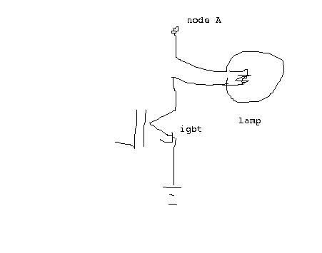
The PWM is generated using a PIC18F2525 and fed into a MOSFET driver in order to amplify the signal. After that, it is fed into the gate of an IGBT.

I've tried multiple frequencies varying from 5kHz to 100kHz with duty cycles from 30% to 70% to no avail.

I've noticed that for a boost converter, there is almost no waste heat output. Only after a couple minutes of operation can I actually notice that the IGBT and MOSFET driver are actually getting a little bit warm.

BoostCircuit.jpg

The circuit I'm using. I didn't bother drawing all the necessary components connected to the PIC MCU. I'm 100% sure the MCU is functioning as it needs to.

BoostGraph.jpg

A screen capture of the oscilloscope. The yellow signal is the waveform of the PWM running at 100kHz with 70% duty cycle. The blue signal is the waveform of the voltage at Node A shown in the schematic above.

Any help appreciated, thanks in advance!
 

boost circuit

Could you provide also Vgs voltage scope picture?

It seems that something is wrong with gate drive or with MOS parasitic capacitances. Some capacities still charge or discharge, that's what you can see on exponential parts of VDS.

If you lower 100R resistor to 10R what happen with these exponential parts ? And also try to put 1k resistor from G to S in close proximity of MOS transistor.

And ALSO it seems that inductor is low value because converter runs at 70% DC and still is in discontinuous mode.
 

boost converter help

yes,it looks like the driving is damped by the 100Ohm.
 

pic boost converter

The waveforms looks completely erratic, even the drive polarity doesn't fit the output signal.
Thus either the parts or the circuit are different than claimed in your drawing.
 

problems boost converter

Interestingly the waveform at the gate of the IGBT looks almost exactly like that of Node A in the schematic.

I desoldered my old IGBT and I soldered in a new one. I tested the IGBT that I desoldered and it no longer works. The new one I soldered in now no longer works either. Could it be that the IGBT I'm using is not powerful enough for this application?

The datasheet can be found here.
 

boost converter

Could it be that the IGBT I'm using is not powerful enough for this application?
Not generally. But you're most likely able to damage the device by considerable over currents. This is mainly a matter of control algorithm and can't be seen from your circuit. You may want to think about a latching over current sense immediately shutting down the IGBT driver. Furthermore, possible problems of circuit layout should be considered.
 

200v boost converter

When I ran it the second time (with the fresh new IGBT), the frequency and duty cycle were 10kHz at 70% duty. If my calculations are right, the peak current should be 8.40A which is below the specified collector current for the IGBT (with a heatsink).

I re-checked the connections in my circuit and cannot for the life of me find any mis-connections. In my schematic I wrote 6A for Ic, its actually at least 10A for temperatures of 25°C.

If you really want to check my control algorithm, it's listed below:
Code:
//Written for MikroC 8.2
void main()
{
   //Power-up timer
   Delay_ms(100);

   TRISA = 0xFF;
   TRISC = 0xF0;
   
   //Enable analog inputs
   ADCON1 = 0x07;
   
   //Initialize the PWM
   PWM_Init(10000); //10kHz
   PWM_Change_Duty(179); //70%

   //Turn working LED off
   PORTC.F3 = 0;
   
   while(1)
   {
      //Stall until the charge button is pressed
      while(1)
      {
         if(PORTC.F7 == 1)
         { break; }
      }
      
      //Continually charge until 200V is reached
      while(1)
      {
         if(ADC_Read(0) < 410)
         {
            PWM_Start();
            PORTC.F3 = 1;
         }
         else
         {
            PWM_Stop();
            PORTC.F3 = 0;
            break;
         }
      }
   }
}
 

how to construct a boost converter circuit

There may be a problem with the calculated inductance.
And change the 100 ohm resistor to 10 ohm.

I myself have not worked much with boost circuits, so cannot say much, but the attachment might help you.
 

driver circuit of mosfet using boost converter

I was looking at my post and noticed that I put a power-up delay of 100ms before I even define the outputs. According to the PIC18F2525 datasheet, the output of the ports are undefined upon start up. Is it possible that because the gate of the IGBT is randomly held high for 100ms, the current exceeds the rated current and destroys the IGBT?

Any thoughts on this theory? I won't be able to test it until Mouser ships me more IGBTs.
 

boost converter problem with a mosfet

Hi DSNet,
It is a possibility, and this is what happened to me a lot earlier, when I was using H-bridges, the MOSFETs accidentally turned on and got burnt, and so, I placed 1k resistors from MOSFET gate to source to prevent accidental turn-on. You should try this, most probably will fix your problem.
This happens because there is a drain-to-gate capacitance in the MOSFET called the "Miller" capacitance. This gets charged sometimes at high voltages and causes the MOSFET to turn on accidentally unless you provide a resistor from gate to source.
 

drawings of boost converter gate drivers

How can one have a 12V 4amps SMPS voltage supply


Thanks
 

boost converter igbt application note

Your scope image does not fit the schematic... could you check everything, cause something is wrong here.

About the pic: at startup the outputs are high-impedance.
So you should use a pull down resistor at the pic output.

Then it could still go wrong: when you configure the CCP you should keep the output high impedance by setting the TRIS bit until the program actually starts running.
 

problem boost converter

hi,
i will suggest you a test method. in the start-up if your controller makes the dutycycle %100 your igbt will dead and you con not even notice it if it wolud not explose :)
so i make my own tests with a "series lamp" always. there is a picture of it, sorry for bad drawing. but you can test your circuit even if your dutycycle %100 at start or igbt was dead. just check the gate waveform or anywhere you want.
the lamp can be a 100W 220V standart house lamp. and if it is turn on there is a problem in the circuit.
remember, you cannot load the circuit with this test structure and maybe your output voltage will be a little bit below the expected voltage. it is just for find the wrong thing.i did not try it on boost converter but i had experiences with lots of switching circuit. so tell me if it is works or not.

93_1248248288.jpg
 

boost converter 200v

I checked out the spec of the ATX and it can probably source around 20A, but your switch can only sink 6A. DC wise you are pulling the DC supply to ground. At initial switch, the inductor current is small so your VA is near ground, but as the inductor current increases, you are seeing voltage drop across your active device. Can you try a much higher rated active device or add a resistor to the output of the PSU to increase its effective output impedance? Try to limit the output current of the supply to about 5A and see what happens.

I am guessing your pwm signal is inverted from the scope at the gate of active device.

Also, consider the effect of the higher than expected current on your inductor vs. its rating.
 

boost converter 200 vdc output

Thank you all for your responses so far.

As it turns out, the 100ms of undefined PWM output was killing the boost converter. I replaced the IGBTs with MOSFETS (IRFP450B) and placed 4.7kΩ resistors pulling the gate down to ground. (Thanks Tahmid)

However, I've run into another problem related to the ADC of the PIC microcontroller. In the circuit, I use a voltage divider of 10kΩ and 1MΩ to step down the voltage going into the analog input by a factor of approximately 100.

Based on the pseudo-code provided below, after I push the start button, the circuit should charge the capacitor bank to 200V and then stop (it does not actively maintain 200V). What happens is that when I push the start button, the PWM will operate for a couple cycles and then stops prematurely because the ADC returns a value that seems higher than 2V. I know that when I feed a DC voltage of 1.95V to the analog input the PWM runs, and stops when I increase that to 2.05V, so I'm pretty sure the code logic works.

I'm not sure if this the right approach, but since the ADC works with DC voltages, but not a rapidly changing one (like the sudden charging of a capacitor), is it possible that the voltage divider adds too much input impedance to the ADC for it to work properly? What can I do about this aside from changing the voltage divider values (I don't want it to be too low or the bank will discharge faster than I want it to)? I'm not all that familiar with ADC modules as this is my first time working with one.

I should note that if I hold the start button down, the circuit will eventually charge the capacitor bank up to 200V, but very slowly since it keeps entering and exiting the loop that controls the PWM module.

New stats:
PWM frequency: 10kHz
PWM duty cycle: 80%
Capacitor bank: Changed from 120uF to 1440uF (Note: it doesn't work on either the 120uF or the 1440uF)
Switch: IRFP450B MOSFET instead IGBT

Code:
//Pseudo-code for the control algorithm
while true
   //2V is the output of the voltage divider at 200V
   if ADC_Read(0) is less than 2V
      PWM_Start();
   else
      PWM_Stop();
      break;
 

Status
Not open for further replies.

Similar threads

Part and Inventory Search

Welcome to EDABoard.com

Sponsor

Back
Top