lily1981216
Member level 4
Hi, the currents of my circuit are large, from 10mA to 60mA. Could someone give me some suggestion about what I should note when I do the layout design. Thanks!
Follow along with the video below to see how to install our site as a web app on your home screen.
Note: This feature may not be available in some browsers.
lily1981216 said:Thanks to all of you! But what does parallel path mean? Does that mean I should use two metal levels to connect the devices instead of one metal level?
jt_rf said:Please make sure the metals are wide enough not only to satisfy the EM checks but also the IR drop on the routing. if there is space constraint you can route it on more than one metals but make sure you put enough vias b/w diff metals.
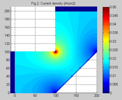
chudong said:but , I have a problem , for the MOS technology, there is a large area for the Power MOSfets, and the metals are not only one layer(at least 2 layers), how should we arrange the metal? (for the current ?)