Continue to Site

Welcome to EDAboard.com

Welcome to our site! EDAboard.com is an international Electronics Discussion Forum focused on EDA software, circuits, schematics, books, theory, papers, asic, pld, 8051, DSP, Network, RF, Analog Design, PCB, Service Manuals... and a whole lot more! To participate you need to register. Registration is free. Click here to register now.

Synchronizers on FPGA

Status
Not open for further replies.

suquid29

Junior Member level 2
Joined
May 2, 2008
Messages
21
Helped
0
Reputation
0
Reaction score
0
Trophy points
1,281
Activity points
1,437
fpga delay line

Hello,

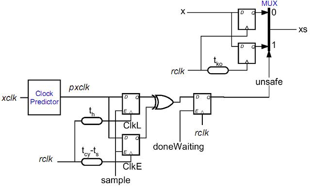
I would like to implement few synchronizers (Plesiochronous, Periodic etc.) on VirtexII-Pro (using VHDL).

1. Can someone point me to where I can find code for synchronizers?
I've tried google but with no luck...
2. What is the best way to implement a configurable delay-line on FPGA?
I've thought of a wide mux with buffers, but the resolution is poor.

Thanks in advanced!
 

delay chains fpga

What is the best way to implement a configurable delay-line on FPGA?

strongly depends on your requirements;
if you need to delay a square wave like clock a configurable pll
will be the best solution [my knowledge of xilinx fpga architecture is
rather poor, but I believe it's similar to altera chips which I work with]

if a random pulse is to be delayed then a solution depends on resolution
and range of delay required;
few but small and 'dense' taps you can achieve connecting the pulse
source to some neighbor input pins and setting different 'intput to array delay'
attribute and then multiplexing them, with some floorplaning results can be
pretty good;

when bigger taps [some ns] are allowed you can rise your input frequency
on internal pll to max. allowed by your fpga and build a kind of 'delay chain'
which means something like this:

Code:
always @(posedge clk)  // POSEDGE
  if ( delay_ctrl == 0 )    delay_chain[max] <= pulse_to_be_dealyed;
  else                      delay_chain[max] <= delay_chain[max-1];

always @(negedge clk)  // NEGEDGE
  if ( delay_ctrl == 1 )    delay_chain[max-1] <= pulse_to_be_dealyed;
  else                      delay_chain[max-1] <= delay_chain[max-2];
etc
what gives half clock resolution;

I think it's possible to use lvds transmitter-receiver pair to do the job
Code:
                 transmitter register
small delay      |0|0|0|0|0|1|1|1|1|0| -> to lvds circuit
big delay        |0|1|1|1|0|0|0|0|0|0| -> to lvds circuit
but have no solution in my head at the moment, just an idea;

and it's also possible to use external, adjustable delay line
 

    suquid29

    Points: 2
    Helpful Answer Positive Rating
fpga synchronizers

I prefer to hear a specification first.
 

fpga configurable delay

Thanks for your replies!

I'll try to be more specific.
Part of a project I'm doing in university, is to implement various synchronizers using VirtexII-Pro.

One example is:


I want to have the ability to create an exact delay (t_i in the drawing) during lab test (by configure register). As much as i've checked, its pretty hard to do, due to the fact that during synthesis and PAR, the tools rout the connections pretty randomly.

My question is how can I control the delay during test, or if this not possible, before PAR, by creating delay lines in the circuit.

Another issue is where can I find VHDL codes for synchronizers (FIFO, Data Delay etc.). I've tried google with no success.

Thanks!
 

sorry suquid but the picture tells me nothing of your requirements;
what's more I'm familiar with xilinx fpga architecture but have
no experience with them;
missing info is the range and step of phase shift you need;
[from your attached picture I guess you need to shift a clock signal
not a random pulse];

first - read carefully DCM description if and how you can shift
phase of the output clock, DCM looks for me as the easiest solution,
your reference clock can be an input to a DCM module, the DCM itself
works as a 'phase shifter' without changing the output frq.;
second - read in ise/virtex manual description of a dll module, such module,
from user point of view, is nothing more then just a delay line;
third - you can force P&R tool to place a specific cell where you want,
see floorplaning section on your tool manual, carefull floorplanig will
allow you to build a delay line as a series of cells the clock signal
has to travel throu and a multiplexer to select desired delay;
and last - if your delay tap can be as big as ~2ns you can use
the solution I've described in the previous post - scan your signal
with both slopes of a fastest clock allowed for your fpga, the scaning
clock you can produce with a DCM module;

where can I find VHDL codes for synchronizers (FIFO, Data Delay etc.)
as far as I know there are no vhdl/verilog codes for fifo, you need to
use tool specific macro [CoreGen in ise case, megawizard for quartus];
no idea what 'Data Delay' is although I guess you mean a kind of
shift register that shifts bytes instead of bits[what means a kind of fifo];
if I'm right such functionality you can build manually if you do not need all fifo features;
 

Status
Not open for further replies.

Similar threads

Part and Inventory Search

Welcome to EDABoard.com

Sponsor

Back
Top