rinaishlene
Junior Member level 3
Hi
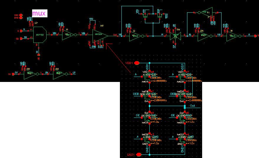
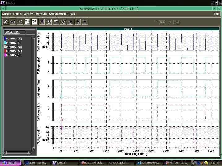
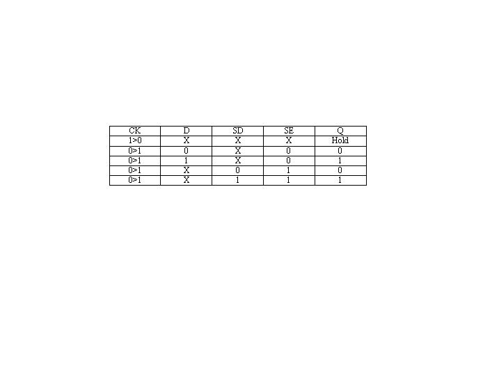
I'm designing a scan D Flip Flop by schematics.The problem is when I simulated the design,the output obtained is delayed by one clock cycle.I'm using Cadence IC Design tool to design the flip flop and using HSPICE to simulate the design.
Is the delay occur because of the design (from the schematic drawn),or from the setup and hold time or any other settting that must be taking place when using HSPICE to simulate the design.
If the delay occur because of the schematics design,would it be better to redesign the schematics by applying Kmap to further simplify the design or redesign the schematics by calculating its logical effort?
")