Continue to Site

Welcome to EDAboard.com

Welcome to our site! EDAboard.com is an international Electronics Discussion Forum focused on EDA software, circuits, schematics, books, theory, papers, asic, pld, 8051, DSP, Network, RF, Analog Design, PCB, Service Manuals... and a whole lot more! To participate you need to register. Registration is free. Click here to register now.

Drain diffusion area is area of the drain diode?

Status
Not open for further replies.

shaq

Full Member level 5
Joined
Jul 23, 2005
Messages
311
Helped
14
Reputation
28
Reaction score
4
Trophy points
1,298
Activity points
3,397
Dear all,

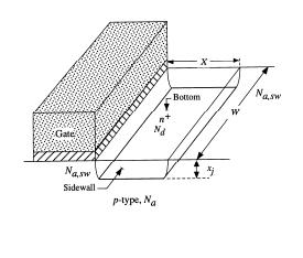
In Hspice manual, I see the different definition of AD.

At "Active Elements" section in Hspice manual, AD is "drain diffusion area."
At "MOSFET Output Templates" section, I see its definition is changed to "area of the drain diode."

Does it mean the same thing?
 

NO; it's wrong

Source and drain areas are defined by diffusing areas on either side of the
gate polysilicon.

g@fsos
 

user raptor1981 wrongly posted reply to report system:

hi, AD is the drain area of MOSFET . AD is not related with the diode area . This can be observed from the model file of AMS , here there are specific models for all elements . For further details please refer to the website ( search by ams )
 

AD, like the others said, is the Drain area (Channel Width * Drain Length). The area of drain diode is the area at the botton of the diffusion plus the area of the difusion sidewalls. The picture gives a better explanation.

100_1268287253.jpg


Added after 1 minutes:

Ps: in the picture the Drain Length is X.
 

Status
Not open for further replies.

Similar threads

Part and Inventory Search

Welcome to EDABoard.com

Sponsor

Back
Top