Continue to Site

Welcome to EDAboard.com

Welcome to our site! EDAboard.com is an international Electronics Discussion Forum focused on EDA software, circuits, schematics, books, theory, papers, asic, pld, 8051, DSP, Network, RF, Analog Design, PCB, Service Manuals... and a whole lot more! To participate you need to register. Registration is free. Click here to register now.

Altium Designer: DRC: Net 3V3 is broken into 4 sub-nets

Status
Not open for further replies.

JohnG300c

Advanced Member level 4
Joined
Dec 5, 2006
Messages
117
Helped
2
Reputation
4
Reaction score
2
Trophy points
1,298
Activity points
2,228
broken-net constraint

I get a "Un-Routed Net Constraint Violation": Net 3V3 is broken into 4 sub-nets. How do i know what nodes are not connected to 3V3?
 

net is broken into 4 sub-nets

Open the "PCB" panel. Select "Rules" at the top of the panel. Select the error in the middle sub-panel. The affected nodes and nets will be listed in the bottom sub-panel.

If you have the boxes checked for Select, Zoom, and Clear Exisiting, the display will zoom to the area of the board when you click on the error or the node/net listing.
 

altium remove rooms

Thanks House Cat. This will highlight the 3V3 net but it does not show me where the net is broken. I have around 100 connections to 3V3 around the board and i have no idea what trace or node is not properly connected to 3V3 (the power plane). Is there a better way than to manually inspect every single highlighted node?
 

altium room violation

Your DRC report should list the exact pads that violate the "Broken-Net Constraint". The listing will have a heading with the netname, then under the netname it lists the pads that the software thinks are disconnected by pad name.

Here's an example of what it looks like for a DRC error that reported "Net VSSA is broken into 6 sub-nets. Routed To 54.55%".

Broken-Net Constraint ( (All) )
Net VSSA
Subnet : C8-2
Subnet : C7-2
Subnet : P2-S5007 P2-B7
Subnet : P2-S5005 P2-B5
Subnet : P2-S5001 P2-B1
Subnet : P2-S5003 P2-B3


You can then use "JC" (Jump to component) to go directly to the error. For the example above, I would use JC, then enter C8, and the error is at pad 2 of C8 when the cursor jumps to that location, etc. You can also use the PCB panel to go to the exact nodes reported in the DRC report - just click on the node name in the bottom sub-panel of the "Rules" display.
 

altium component class

Thanks House Cat. I assume you refer to the HTML report which never comes up on my system. I had previously installed AD in a different directory and the new installation for some reason tried to find the report templates in the OLD installation directory. I have not yet figured out where the template installation directory setting is stored (i have checked the registry and the file system without luck). I'm therefore just using the messages pane for the DRC output which doesn't contain any subnets. Anyways, i have gotten rid of all DRC errors except certain components that are not PLACED in the room it was created in (i.e. their schematics name). Any idea how to "unassign" a component from a room?
 

altium net class pcb rule

The location of the DRC report templates is set in your preferences. Hit "OP" to bring up the PCB Editor Preferences page. Go to Preferences>PCB Editor>Reports, and you will see the table of templates and the check boxes to select which reports get generated. You can set everything from this page of the preferences.

Components are assigned to component classes which are then assigned to rooms by design rules in the Placement>Room Definitions section. You can edit the component classes from the PCB Panel. Select "Components" at the top of the panel. Then double click on the component class that contains the component you want to remove from the room. An editing dialog will come up, and you'll see the arrows that allow you to move components in or out of the class that defines the room. You can also get to the same editing window from the menu Design>Classes by clicking on the name of the component class that contains the component you want to add or remove from the room.
 

how to delete room in altium pcb

Thanks a million House Cat. My design is pretty much clean now :)

Added after 2 hours 8 minutes:

House Cat, one more thing...

I now notice that certain components are stuck in component classes and when i do an ECO from schematics AD wants to reassign the components to the old component classes again. I tried to update the schematics while in the PCB editor. 15 differences were detected (the components that were removed from the component classes) but i was unable to create an ECO back to schematics from the "differences dialog". I instead got a dialog where it says "differences detected but no ECO generated. Please review the project options.".

Of course, i couldn't find any useful project option...
 

altium designer broken net constraint

The Project Option setting that the software is trying to tell you about is found on the "Class Generation" tab of Project Options.

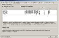
There are check boxes for selecting how the software automatically assigns components to classes and rooms. Look at the third column of the table - if you have the boxes checked to generate component classes and rooms from the schematic pages, it will automatically assign the components to a class and then assign the class to a room. This would try to override the changes you made manually to the PCB class assignments.

If you want to force a component into a particular class, you would check the box at the bottom of the tab where it says "User-defined Classes>Generate Component Classes". You would then define a new parameter for the component called "ClassName", and give it a value equal to the name of the class. For a large number of components, you would want to use 'Tools>Parameter Manager' to add and manage component classes.
 

broken-net constraint ( (all) )

Thanks House Cat. I'll try your suggestions :)
 

altium designer 6 emplates

House Cat, despite having created a "ClassName" parameter set to "NONE" for all components i want to place outside their default rooms AD wants to force the components in question back to the original class name when i do an "Update PCB Document...".

I also get the same result when trying to update the schematics from the PCB error (...no eco generated...).

Am i missing something here...?
 

altium highlight net

What boxes do you have checked on the "Class Generation" tab of Project Options?
 

is broken into 22 sub-nets.

I have uploaded an image of the dialog:
 

net is broken into 2 sub-nets

From your posted picture, you have given the software two instructions to follow. First, place all of the components on a particular schematic sheet into the same room. Second, that you will define rooms for components in addition to the automatic assignment of rooms.

If you don't assign a class to one of your components, then the software will assign it to the default location. Instead of assigning a blank parameter, give your user ComponentClass parameter a dummy value of something like N1, N2, etc.

If you aren't using rooms for anything on the PCB, then you can remove them completely by unchecking the boxes in the "Generate Rooms" column of the Schematic Sheets table. When you compile the schematic and send it to the PCB you'll generate an ECO that will remove the room assignments.

If you're not using your rooms for design rules that would prevent it, you could also edit the shape of your rooms to include the extra components.
 

broken-net constraint

Thanks House Cat. The problem seems to be that AD wants to assign the components to the class they were deleted from DESPITE the fact that the components were assigned a new class via the ComponentClass parameter (set to "NONE" for all these components). It seems like the ComponentClass "override" method doesn't work.
 

net is broken into 2 sub-nets

If you look in the documentation, you will find that the proper parameter name to assign a component to a class is "ClassName". I just tried reassigning several components to the room "NONE" on the project that I am working on, and it does, indeed, work. Without looking at your specific project, I'm not sure what you may be doing wrong.
 

is broken into 2 sub-nets

Thanks House Cat. I'll just ignore this issue for now. In the worst case, i'll by mistake update the PCB and forget to uncheck the component group updating which will make certain components "green" on the PCB. This will not affect the end result.
 

is broken into 15 sub-nets

JohnG300c said:
I get a "Un-Routed Net Constraint Violation": Net 3V3 is broken into 4 sub-nets. How do i know what nodes are not connected to 3V3?

Hi,
I met similar problems.
and my labmate helped me to solve it.
My error is that surface component is on top layer. But I used bottom layer wire to connect it. so that's all.
Thanks.
 

Status
Not open for further replies.

Part and Inventory Search

Welcome to EDABoard.com

Sponsor

Back
Top