ericmar
Full Member level 5
Dear All,
I have been trying to learn more about interfacing with a differential input ADC. I happened to find the following information.
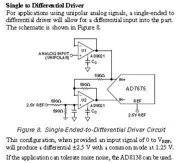
However, I do not quite understand what it means by "This configuration, when provided an input signal of 0 to Vref, will produce a differential ±2.5V with a common mode at 1.25V."
1. Why is the differential ±2.5V and the common mode 1.25V?
2. What if the reference voltage is not 2.5V but 1.5V?
3. What happen if the +Input signal of U2 is not the same as the Reference voltage supplied to the AD7675? How does it affect everything?
4. Notice that one end of the 2nd 590Ω resistor at the +Input signal of U2 is connected to different ground as others. Why is it so?
5. How to calculate the resistance value?
By the way, my design is to convert a single-ended output signal, which is from a DAC, to a differential input ADC.
Please advice if are experience in this.
Thanks in advance.
Regards,
Eric
I have been trying to learn more about interfacing with a differential input ADC. I happened to find the following information.
However, I do not quite understand what it means by "This configuration, when provided an input signal of 0 to Vref, will produce a differential ±2.5V with a common mode at 1.25V."
1. Why is the differential ±2.5V and the common mode 1.25V?
2. What if the reference voltage is not 2.5V but 1.5V?
3. What happen if the +Input signal of U2 is not the same as the Reference voltage supplied to the AD7675? How does it affect everything?
4. Notice that one end of the 2nd 590Ω resistor at the +Input signal of U2 is connected to different ground as others. Why is it so?
5. How to calculate the resistance value?
By the way, my design is to convert a single-ended output signal, which is from a DAC, to a differential input ADC.
Please advice if are experience in this.
Thanks in advance.
Regards,
Eric