Continue to Site

Welcome to EDAboard.com

Welcome to our site! EDAboard.com is an international Electronics Discussion Forum focused on EDA software, circuits, schematics, books, theory, papers, asic, pld, 8051, DSP, Network, RF, Analog Design, PCB, Service Manuals... and a whole lot more! To participate you need to register. Registration is free. Click here to register now.

What is the cause of distorting in my circuit?

Status
Not open for further replies.

Veriloger

Newbie level 4
Joined
Mar 12, 2012
Messages
7
Helped
1
Reputation
2
Reaction score
1
Trophy points
1,283
Activity points
1,379
Hi,

I have the following waveform coming out of a MOSFET driver. As shown as red in the image. How do i go about cleaning up the signal without loosing the sharp rise/fall times? The very sharp rising/falling edges are important, which is why i don't want them to slow down.

In this circuit, i have the output of the driver connected to the gate of an Nch MOSFET via an AC coupling capacitor, a zener (tying gate to source), a resistor (tying gate to source). The traces between each component lead is only a few millimetres long. The longest being from the AC coupling capacitor and the gate of the MOSFET, which is less than 20mm. What are the likely suspects to the cause the distortion?

Also what is the cause of the spikes just before each transition? Is this just internal inductance of the driver?
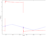
signals.png


Thanks
 

Hi,

it is unclear where in your described schematic you had the measurement points.
It is also unclear what "distortion" you mean.
Usually you don´t need an AC coupling capacitor.
What driver are you using?

--> show us your schematic and give timing information. (pulse duration = 0.5us? frequency about 1MHz?)
****
If with "distortion" you mean the non horizontal lines in the red line:
Then there are many sources for this:
* bootstrap capacitor is loosing voltage (quite normal)
* your scope probe is not adjusted
* your scope probe GND is not good placed
* your AC coupling capacitor generates this waveform

The spikes before the transition should be caused by the driver input signals - at least in my eyes.

All in all the waveform is not that bad.

Klaus
 

The measurement point is directly on the output pin of the driver with the ground as close to the driver as possible. The oscilloscope probe using a spring ground clip at the tip instead of a cable clip.


The output of the driver is supposed to be a step between 0 and 12 volts. Distortion being overshoot and ringing. If the circuit was critically damped with no distortion the decay to 12 volts wouldn't exist.

The AC coupling capacitor because gate driving signal is level shifted. Hence why i stated drain and source of the MOSFET with no voltages.

The triangular wave in blue is the input waveform at 800kHz with a 50% duty ratio. The ringing on the input waveform is only seen when the driver and the MOSFET is turned on. By turning on the MOSFET, i mean applying a voltage across the drain-source. The ringing on the input waveform is only about half that seen here when only the driver is turned on. Previously, I have been applying square wave step inputs in to the driver via an FPGA source but i was curious about whether the driver was some form of analog amplifier or whether it operated like a Schmitt trigger - hard on, hard off - hence the triangular wave to drive such a device/circuit. As i'm attempting to figure out where the overshoot and ringing is coming from.


The waveform is awful for my application. Once i sort this out, i want each pulse to have a width of approximately 5ns. Which, i currently can't obtain.
 

In any CMOS inverter, if you look close enough, you'll see
such opposing-direction perturbations precede the output
going in the eventual right direction. This is the Miller
capacitance of the FET coupling the (say) L-H gate transition
to the output, ahead of the eventual H-L drain transition.

You also have that huge taper chain's shoot-through
current and gate displacement currents banging the ground
and the supply, and through the local decoupling one of
those has a pretty strong dynamic effect on the other.
All of that spike-ery bumping against the ground inductance
to produce voltage spikes on the 'scope probe, by jacking
the reference ground (but also the MOSFET driver's internal
vs reference ground, the output will follow the on-chip
ground which has additional wire bond inductance and is
never as clean as board ground).
 

Hi,

The waveform is awful for my application.
Does this mean it decreases your applicationn's performance? Or does it just look awful?

For the mosfet it should be no problem. The mosfet will be safely ON with maybe 8V so ringing around 11.5V to 12.5V won't change performance.

Klaus
 

Status
Not open for further replies.

Similar threads

Part and Inventory Search

Welcome to EDABoard.com

Sponsor

Back
Top