Continue to Site

Welcome to EDAboard.com

Welcome to our site! EDAboard.com is an international Electronics Discussion Forum focused on EDA software, circuits, schematics, books, theory, papers, asic, pld, 8051, DSP, Network, RF, Analog Design, PCB, Service Manuals... and a whole lot more! To participate you need to register. Registration is free. Click here to register now.

High Voltage Buck Converter

Status
Not open for further replies.
you got the point!
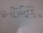
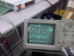
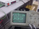
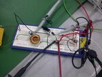
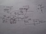
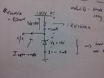
you can use 2183 just like 2117 with low side gate output not connected and connecting Lin to GND or Vcc.
 
I had no problems to imagine the purpose of the moved Rg. But I didn't see the undershoot protection in this "extreme" way yet. Thanks for clarifying. I would probably provide both resistor options (Rg and Rs) and check for the actual switching node undershoot in your circuit.

You didn't yet comment my first statement about possible boostrap failure.

FvM,

Thanks for your reply. I totally agree with you on how the high duty cycle (D) would disallow the bootstrap capacitor to charge because whenever we slowly increase, increase, increase the ON time for the main FET (which also increases the D), we are actually reducing, reducing, reducing the OFF time in a given switching period or frequency. And since the bootstrap capacitor only has the "chance" to charge up during main MOSFET = OFF (eg: OFF time), by increasing the ON time so much (that is, decreasing the OFF time), the bootstrap capacitor might not be able to charge to the voltage we want, and hence Vgs <15V and the system may fail. While all these have not included the propagation delay, rise/fall time and etc...

The only solution I could think of is to relocate the gate resistor back to the position between o/p of the gate driver and gate, and parallel it with a diode to it.

This method could:

1) reduce the charging time for the bootstrap cap since i relocated the Rgate back to its original position (away from the bootstrap charging up path)

2) reduce the turn-off time for the main FET by allowing the majority of the gate charges to flow "away" through the newly added diode instead of Rgate, hence allowing the bootstrap cap to start charging earlier

How do you think if my method is feasible?
 

Reviewing your initial post, I see that you intend a 100 to 28 V converter. In this case, high duty cycle won't be an issue, if the PWM controller implements a duty cycle limiting means.

The other possible problem is however low or even no load, resulting in DCM (discontinuous mode) operation. Diode conduction time will be very low, at no load, the diode possibly doesn't switch on at all. Imagine a load current step to zero, the output voltage does a small overshoot, compensated by a long duty cycle 0 period. If the bootstrap capacitor discharges in this phase, you need to completely shut down the output voltage to restart the converter.

My coclusion is, that reliable operation can't be achieved without either a synchronous low-side switch or an auxilary charge pump to supply the bootstrap circuit.
 

As FvM pointed and I wrote before,using a low side mosfet is the best option.(you need just one low cost mosfet instead of FW diode and the driver is there waiting to drive it!)

1-more efficiency
2-No bootstrap charge problem
3-No "no load" overshoot .

Regards
 

I am starting to know more of your point.

Put it this way, could we assume that for a pure resistive load for example, the load resistance increases towards a light load condition (which also means infinite load resistance or open circuit under no load), and the resistance decreases towards a heavier load situation.

And since the main inductor does not allow the load current to change abruptly, but the load's resistance can do so. That is, for example, as what you've said load current step to zero (meaning load resistance step to infinity)

v(t=0-) = i(t=0-)*R
i(t=0-) = i(t=0+) <-- no change in magnitude of current since heavy inductance

Therefore v(t=0+) will be expected to increase to infinity since R jumps to infinity as well, however, there is a bypass capacitor coupled to the o/p terminals and hence under a practical scenario, the overshoot will definitely still occur but would be contained to prevent it from shooting infinitely. And how much o/p voltage overshoot will be depending on the values of L and Cout practically, or could be calculated out theoretically using the transfer function model?
 

Dear guys,

I've just built up my non-synchronous Buck converter. Both the schematic and the actual prototype on breadboard are attached.

After some testings, I am glad that the Buck is working from the range of duty cycle, D = 3% to 97% w/o the system going unstable. Although my orginal intention is to step down a 100V to 28V, I've put HV DC = 30V only for testing purposes. The step down ratio should be the same.

However one problem which I wish to clarify is when I was checking out the waveform of my Vs w.r.t. GND, could anyone explain why the Vs waveform has a single hump before it floats correctly to 30V. This phenomenon was also observed when I've measured the gate voltage (Vg, not Vgs) w.r.t. GND as well.

Could anyone advise what's wrong with here? Thank you.

Inductor datasheet (Model no. 2200LL-471-RC: http://www.bourns.com/data/global/pdfs/2200ll_series.pdf)
nMOS datasheet: (http://www.irf.com/product-info/datasheets/data/irf640n.pdf)
 

Attachments

  • IMG-20111216-00478.jpg
    IMG-20111216-00478.jpg
    1.7 MB · Views: 90
  • IMG-20111216-00477.jpg
    IMG-20111216-00477.jpg
    1.8 MB · Views: 84
  • IMG-20111216-00476.jpg
    IMG-20111216-00476.jpg
    1.6 MB · Views: 82
  • IMG-20111217-00484.jpg
    IMG-20111217-00484.jpg
    1.4 MB · Views: 79
Last edited:

could anyone explain why the Vs waveform has a single hump before it floats correctly to 30V.
There's nothing wrong, it's a regular DCM discontinuos mode buck converter waveform, as observed at low output loads.

Strictly spoken, the "bump", more exactly a sine shaped oscillation, doesn't occur before the converter "on"-period (which is surely not a floating state). It happens after the diode conduction phase, when the diode disconnects and the switching node is actually floating. You get a low energy oscillation, frequency is defined by the converter inductance and transistor + diode capcitance. Nothing to worry about.

More problematic in terms of generated interferences is the high frequency oscillation during transistor switch-on. But looking at your breadboard design and probe connection, it's not surprizing and doesn't necessarily represent the behaviour of the buck converter itself.
 
Ok guys, now I've new problem. I've switched the duty cycle till 50% to allow the Buck operates in the CCM. And I've replace the HV DC rail with a High voltage DC PSU.

Upon ramping the HV DC rail slowly to 100V, I've noticed after Vdc > ~80V, to my horror, the Vgs starts to increase as well. It climbed till about > 20V (which is the Vgs(max) specified in the datasheet) and therefore I do not dare to increase my Vdc = 100V.

Could anyone knows why is this so?

And also, the increment of the Vgs was not the first observation made. The Vgs starts to transient and the transient magnitude increases with Vdc.
 

Attachments

  • IMG-20111219-00485.jpg
    IMG-20111219-00485.jpg
    1.7 MB · Views: 79
  • IMG-20111219-00486.jpg
    IMG-20111219-00486.jpg
    1.7 MB · Views: 73

I wonder how you are measuring Vgs? You'll need a differential probe which apparently isn't used in your measurement. If you ground the switching node by the oscilloscope probe, other unwanted effects may occur.
 

I wonder how you are measuring Vgs? You'll need a differential probe which apparently isn't used in your measurement. If you ground the switching node by the oscilloscope probe, other unwanted effects may occur.

Spot on, I did experienced problem with the system when I just used a single channel to measure Vgs, that is connecting the main probe to Gate and the black clip of the probe to Source. That doesn't work for an unknown reason.

So what I did was, to use two probes instead, one to Gate, one to Source and I set the o-scope to display CH1-CH2 waveform. Hence if you looked at the attached photos, you'll see the maths option being lit up, instead of CH1 or 2.

That is how I study the Vgs waveform. Did I do it wrongly?
 

you'll see the maths option being lit up, instead of CH1 or 2.
I see it when I know it.

Differential is basically O.K., but the proble compensation may be slightly wrong. You would want to check it first by connecting both probes to the same test point. If you can verify correct differential measurement, than the Vgs value should be expedcted correct. It's however easy to get parasitic effects in the breadboard setup. It may be necessary to connect a z-diode across the bootstrap capacitor.

Thanks for your great suggestion, in fact, this is my idea too.

However, do you think it is more appropriate to attach the z-diode as close as possible to the MOSFET gate-source terminal (since this is the protection of interest) or as you mentioned, attach it in parallel with Cbst as to ensure the voltage to supply Vgs is always rated to the z-diode rating? Or in fact, both should yield the same results?
 

Connecting the z-diode directly to gate-source has advantages and disadvantages. The disadvantage is adding capacitannce and slow down switching speed. But it can be compensated by reducing Rg, if necessary. O.K. considering the breadboard setup, it's probably safer to place a 15 to 18V z-diode near the FET.
 

Connecting the z-diode directly to gate-source has advantages and disadvantages. The disadvantage is adding capacitannce and slow down switching speed. But it can be compensated by reducing Rg, if necessary. O.K. considering the breadboard setup, it's probably safer to place a 15 to 18V z-diode near the FET.

Ok, I'll add a 15V z-diode across my gate/source tomorrow. But on other hand, would this z-diode, solve the transient issues, or as you've mentioned. This transient is most probably generated from the parasitic effect from the breadboard, and therefore, if this circuit is built on a stripboard as example, this transient effect would not be there.

Or do you think I should add a RC snubber which is always good for eliminating transient phenomenon.
 

Reviewing your initial post, I see that you intend a 100 to 28 V converter. In this case, high duty cycle won't be an issue, if the PWM controller implements a duty cycle limiting means.

The other possible problem is however low or even no load, resulting in DCM (discontinuous mode) operation. Diode conduction time will be very low, at no load, the diode possibly doesn't switch on at all. Imagine a load current step to zero, the output voltage does a small overshoot, compensated by a long duty cycle 0 period. If the bootstrap capacitor discharges in this phase, you need to completely shut down the output voltage to restart the converter.

My coclusion is, that reliable operation can't be achieved without either a synchronous low-side switch or an auxilary charge pump to supply the bootstrap circuit.

Hi FvM,

I am satisfied that the HCPL-3180 Avago optocoupler works as well as the IR2117 gate driver. In fact, I could have a pulse with peak amplitude of only 3.3V to the photodiode by tweaking the optocoupler series resistor. And I just love the optocoupler because it does not need any Vcc (IR2117 does), but only a bootstrap configuration.

Attached are my circuit connections (still using breadboard though for testing). Also, I've used a 10V z-diode to clamp V(gs).

Ok, here comes my next challenge as well as a little problem. In my past various testings, I've used a stand-alone low voltage DC PSU (10V) to provide the necessary source to charge up my bootstrap capacitor periodically. I would now like to remove that, and utilise power from the HV 100V DC rail instead (see Otpo_noLVPSU.jpg).

I still really do want to continue to utilise the bootstrap config but instead of using a separate unit, a LV 30V(max) DC PSU to supply the bootstrap charge momentary, I would now like to obtain the charge or current from the 100V High DC rail. By doing this, I could simulate a more realistic situation because, ultimately at the end of the day, there would be only a 100V DC battery supplying power to all the sub-system, including the boostrap supply.

As necessary, I've first done my research about auxiliary power supply concept and now that I share to hope to get more insights from members with good experience over here:

100kΩ resistor in series with 10V z-diode:

As seen in zener_setup.jpg, R=100kΩ in series with a zener of V(bk-dn) of 10V, therefore V(R)=100-10=90V. I(z)=V(R)/R=90/100k=0.9mA.

I've constructed the schematic on a breadboard as shown in zener_breadboard.jpg. I've chosen R = 120kΩ and z-diode 1watt 1N4740AC.

The 100V DC supply is then connected to the top part of the 120kΩ resistor and the zener reverse voltage is being recorded by an oscilloscope as shown in zener_oscope.jpg, with a reading of ~9.886V.

Here comes my question, if I connect this regulated 10V to my optocoupler as a replacement for the LV DC PSU, would the circuit readings change? What I believe is that this optocoupler would draw some average current, and hence in turn, changing the current flowing through the 120k resistor, that is, I(R)=I(z)+I(optocoupler). So to find out how much current will the optocoupler draw, I've measured with the original setup (the one with LV PSU to supply the bootstrap cap charge), the avg. current is about 7.10mA (see Optocoupler_Iin.jpg).

So will this work as a substitute for a separate LV PSU for charging the bootstrap cap?
 

Attachments

  • IMG-20111222-00491.jpg
    IMG-20111222-00491.jpg
    1.9 MB · Views: 71
  • opto_noLVPSU.jpg
    opto_noLVPSU.jpg
    1.7 MB · Views: 82
  • zener_setup.jpg
    zener_setup.jpg
    1.4 MB · Views: 74
  • zener_breadboard.jpg
    zener_breadboard.jpg
    1.9 MB · Views: 88
  • zener_oscope.jpg
    zener_oscope.jpg
    1.5 MB · Views: 71
  • Optocoupler_Iin.jpg
    Optocoupler_Iin.jpg
    1.7 MB · Views: 78

Typical HCPL-3180 supply current is about 3 mA (< 6 mA), you should add several mA for MOSFET gate charge multiply 100 kHz.
 

Typical HCPL-3180 supply current is about 3 mA (< 6 mA), you should add several mA for MOSFET gate charge multiply 100 kHz.

Yup, I've did that by reducing the value of the resistor connected in series and the bootstrap resistor.

IRF640N gate charge is about 42nC at Vgs=~10V. Using your formula, additional mA = 42X10^-9 X 100X10^3 = ~4.2mA

So, do you mean I should add additonal of 4.2mA on top of the zener current?

That means, if the zener current is 50mA, I must size the zener resistor such that it allows 50mA + 4.2mA of current to flow through?
 

The problem is the series resistor power loss. You should at least provide 10 mA.
 
Hi guys,

I've managed to solder the high current part of the circuit on the stripboard so that I could run it on high current (up to 3.6A DC at o/p).

The rest of the circuit was still made on breadboard because the current rating is not high (in mA range) (see attached). Did a high current test and was happy that it is successful. However I've seen that the o/p voltage has spikes which is rather high (see attached).

I thought I've already included a smoothing capacitor which is the 150uF capacitor (see orginal circuit in previous post), could anyone advise why there is still spikes going on?

Should I add in a RC snubber to suppress these transients?

Thank you.
 

Attachments

  • buck on stripboard.jpg
    buck on stripboard.jpg
    170.1 KB · Views: 78
  • Buck on stripboard oscope.jpg
    Buck on stripboard oscope.jpg
    87.5 KB · Views: 76

Status
Not open for further replies.

Similar threads

Part and Inventory Search

Welcome to EDABoard.com

Sponsor

Back
Top