Continue to Site

Welcome to EDAboard.com

Welcome to our site! EDAboard.com is an international Electronics Discussion Forum focused on EDA software, circuits, schematics, books, theory, papers, asic, pld, 8051, DSP, Network, RF, Analog Design, PCB, Service Manuals... and a whole lot more! To participate you need to register. Registration is free. Click here to register now.

[SOLVED] Mosfet as switching circuit

Status
Not open for further replies.

Linspire

Full Member level 5
Joined
Sep 1, 2011
Messages
303
Helped
1
Reputation
2
Reaction score
1
Trophy points
1,298
Location
M'sia
Activity points
3,279
Guys,
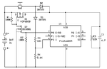
I'm trying to implement power saving mode for my embedded circuit design.
There are several external hardware which will be running together with microcontroller.
1.RFID reader
2.LCD
3.SD card
4.MAX-232

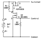
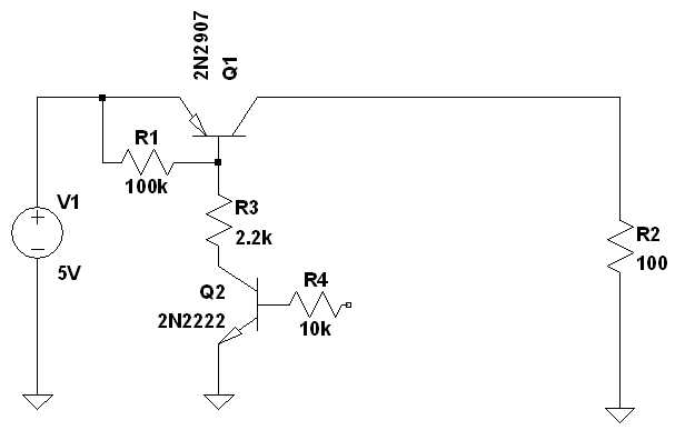
I have tried built IR610MOSFET N-type circuit to turn on/off for external hardware when PIC's in sleep mode by sent a signal high to the MOSFET's GATE.
However, this mosfet required high voltage to turn on the circuit.
My overall external circuit can be work within 4.2V.
I have measure the high signal voltage from PIC's pin is around 4.6V.
I have tried to built with two BJTs, however there isnt sufficient voltage for the load (external hardware).

So anyone has this kind experience ?


Regards
Linspire
 

Why not switch to a logic-level, P-channel, power MOSFET for high side switching controlled by a small logic-level, N-channel MOSFET or an NPN transistor driven from your microcontroller. How much current is required for each device.

Ken
 

Hi, current required for each devices is
1. RFID reader : 30-40mA, minimum voltage to operate is 4.0V
2. LCD :10mA
3. Max-232 : a very small current flow; maybe few microA

And I'm using rechargeable battery 5V.
I have tried driven using NPN transistor,however it is insufficient voltage (3.5V) for load (RFID reader) to operate it.


Linspire
 

Sounds like you are using an unsuitable configuration of the switching transistor. We would usually utilize a PNP transistor (or a PMOSFET, as suggested) to switch a positive supply. Both will allow a very low (e.g. < 50 mV) voltage drop.
 

I designed the attached circuit to provide push-on/push-off/program-off for a microcontroller. You could use the Q1/Q2/R1/R2 circuit to switch power to other devices.

Ken
 

Attachments

  • PicaxePowerSwitch3V.gif
    PicaxePowerSwitch3V.gif
    17.5 KB · Views: 134
  • Like
Reactions: nmbg011 and FvM

    FvM

    Points: 2
    Helpful Answer Positive Rating

    nmbg011

    Points: 2
    Helpful Answer Positive Rating
Sounds like you are using an unsuitable configuration of the switching transistor. We would usually utilize a PNP transistor (or a PMOSFET, as suggested) to switch a positive supply. Both will allow a very low (e.g. < 50 mV) voltage drop.

Do you have sample schematic diagram so that I can do in multisim simulation ?


Linspire

---------- Post added at 23:00 ---------- Previous post was at 22:59 ----------

I designed the attached circuit to provide push-on/push-off/program-off for a microcontroller. You could use the Q1/Q2/R1/R2 circuit to switch power to other devices.

Ken

Erm,I cant truly understand the schematic diagram you attached.
Sorry, I'm not very good in mosfet usage.


Linspire
 

The attached is the minimum circuit, Q1 is a P-channel logic-level MOSFET with the Source (S) to the battery +. Q2 is an N-channel logic-level MOSFET with its Source connected to battery common (-). Drains (D) and Gates (G) are connected as shown. Control is a low (off) or high (on) from the microcontroller.

A high on Q2's gate turns on Q2 and pulls Q1's gate to common. This turns on Q1 and supplies battery power to its Drain and to you devices. A low on Q2's Gate turns Q2 off. That allows R1 to pull Q1's gate to B+ and turning it off. That cuts power to Q1's drain and to your devices.

Ken
 

Attachments

  • PicaxePowerSwitch3V 01.gif
    PicaxePowerSwitch3V 01.gif
    7 KB · Views: 98
Last edited:
You use a PNP transistor for Q1 and PNP for Q2, if you add base series resistors, e.g. 1 - 2 k for Q1 and 10 - 20 k for Q2.
 

The attached is the minimum circuit, Q1 is a P-channel logic-level MOSFET with the Source (S) to the battery +. Q2 is an N-channel logic-level MOSFET with its Source connected to battery common (-). Drains (D) and Gates (G) are connected as shown. Control is a low (off) or high (on) from the microcontroller.

A high on Q2's gate turns on Q2 and pulls Q1's gate to common. This turns on Q1 and supplies battery power to its Drain and to you devices. A low on Q2's Gate turns Q2 off. That allows R1 to pull Q1's gate to B+ and turning it off. That cuts power to Q1's drain and to your devices.

Ken

Are you saying at "switched" point , it will be connected to my load (RFID reader, max-232) ?


Linspire

---------- Post added at 23:36 ---------- Previous post was at 23:34 ----------

You use a PNP transistor for Q1 and PNP for Q2, if you add base series resistors, e.g. 1 - 2 k for Q1 and 10 - 20 k for Q2.

Two PNPs ?
So the load will be connected to the collector(C) ?
And there is no resistor on emitter for both PNP, only series resistors on base(B).

Linspire
 

I have tested using multisim as FvM suggested, but the result is unsatisfied.

PNP_NPN.PNG

4.5V is driven by my microcontroller.
let assume my load is 100ohm.
5V is my battery.


Linspire
 

Right now I simply put power Mosfet P and N type.
I got negative voltage and negative current which shown below:
PNP_NPN_1.PNG


Linspire
 

I designed the attached circuit to provide push-on/push-off/program-off for a microcontroller. You could use the Q1/Q2/R1/R2 circuit to switch power to other devices.

Ken


Sorry what is PICAXE ?
 

Your battery is backwards. The 2N7265 is not a logic-level Mosfet.

Ken

Can you provide appropriate model which available in the market ?


Linspire

---------- Post added at 10:59 ---------- Previous post was at 10:46 ----------

I wasn't aware of so much ways to mess up a simple circuit.


Which point connected to which components ?

Linspire

---------- Post added at 11:57 ---------- Previous post was at 10:59 ----------

For FvM 's schematic diagram,
I have tested the circuit, however even 1V to controlled point can give 4.5V. Only there is 0V turn off the circuit.

And,by the way how does this circuit truly operate ?
Is it same explainantion by KMoffett .


Linspire
 

What simulator are you using? I have no idea what spice models you need, so Google:logic level mosfet model
The various manufactures should have them available. The MOSFETS I used were a from Mouser Electronics

FvM's circuit operates the same as mine. His turns on at any control voltage above ~0.6V. His requires continuous drive current to the transistor. Mine requires ~3V to turn on, but requires no continuous drive current.

Ken
 

How to say, continuous drive current to transistor ?
Will this be wasting the battery lives usage ?
I'm using Multisim to simulate.


Linspire
 
Last edited:

I agree, that MOSFET are preferable in terms of efficiency. But Linspire has been asking explicitely for a bipolar transistor circuit. In those cases, where the supply current doesn't vary too much, the additional base current can be almost neglected with a correctly dimensioned circuit.
 

Status
Not open for further replies.

Part and Inventory Search

Welcome to EDABoard.com

Sponsor

Back
Top