Continue to Site

Welcome to EDAboard.com

Welcome to our site! EDAboard.com is an international Electronics Discussion Forum focused on EDA software, circuits, schematics, books, theory, papers, asic, pld, 8051, DSP, Network, RF, Analog Design, PCB, Service Manuals... and a whole lot more! To participate you need to register. Registration is free. Click here to register now.

How to set the signal output wave port size?

Status
Not open for further replies.

John_li

Full Member level 5
Joined
Aug 6, 2005
Messages
272
Helped
9
Reputation
18
Reaction score
1
Trophy points
1,298
Activity points
2,945
Hi friends,
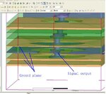
As attached photo,I want to set wave port size of signal output.For this type is the coplanar mixed with stripline,how set the wave port size,W=?H=?(the trace parameter width=150um,H=204um).
Thanks in advanced,
 

Attachments

  • 1.JPG
    1.JPG
    97.5 KB · Views: 156
Last edited:

I think it's not very difficult,so you can use parametric sweep to get the best size of your feeding.
 
I think it's not very difficult,so you can use parametric sweep to get the best size of your feeding.

What? Let's try to think, instead of trial and error.

The port area needs to cover the signal conductor and the corresponding ground returns.
 

...any stripline has the waveport extending from top gnd to bottom gnd and extend left and right ~7*width of trace (rule of thumb, not law of land...)

have fun
 
hi
how many ground u have ? why u want to use wave port try lump element?
 
hi
how many ground u have ? why u want to use wave port try lump element?
I want to calculate the port impedence and the IL of path

---------- Post added at 00:19 ---------- Previous post was at 00:16 ----------

...any stripline has the waveport extending from top gnd to bottom gnd and extend left and right ~7*width of trace (rule of thumb, not law of land...)

have fun
What confuse me is the left and right sides have ground plane?whehter have different setting ?
 

hi
i confused .how was your structure ground ? are u have CPW structure?
 
It is multi-layer PCB for mobile.And microstrip is designed in internal layer.
 

Status
Not open for further replies.

Part and Inventory Search

Welcome to EDABoard.com

Sponsor

Back
Top