Continue to Site

Welcome to EDAboard.com

Welcome to our site! EDAboard.com is an international Electronics Discussion Forum focused on EDA software, circuits, schematics, books, theory, papers, asic, pld, 8051, DSP, Network, RF, Analog Design, PCB, Service Manuals... and a whole lot more! To participate you need to register. Registration is free. Click here to register now.

How to clip (define) the output signal?

Status
Not open for further replies.
FvM:
Sorry, but I don't fully understand your post #19. Could you clarify and/or proposed me any circuit, please? :idea:

Barry:
1) The PROPOSAL_1 is really yours (take a look to post #2 ;-)). But,... what would I need to make it Linear? :-|

2) So, if in PROPOSAL_2 do I change R1 by this Simple Current Source; will it be linear then? 8-O
89_1315598530.jpg


Thanks! :-D
 
Last edited:

I don't fully understand your post #19.
It's very simple. The red plot shows the R-to-V characteristic of any voltage divider circuit, that implements endpoints of 0.5 and 9.5 V e.g. the said proposal 1 and 2. The blue plot shows a linear circuit with current source. The plots visualize the simple fact, that you can't have both linear characteristic and 0 to infinity resistance range.

In my opinion, you have to decide about the intended characteristic before thinking about circuit details.
 
For a given range of resistance it will be linear (theoretically). Since the current is constant regardless of load, the output voltage will be V=I*R. In others words, voltage will be linear with respect to resistance. But we don't really know all your requirements. For example, if
youre going to do an analog/digital conversion and read it into a processor you can save expense and let the software do the linearization.
 
Barry:
What do you mean that I can save expense and let the software to do the linearization?
If I use a Non-linear system, I will need to calculate the non-linear output transfer function, anyway for the software, isn't?

By the way, I added the resistor (R2) suggested for PROPOSAL_2 (between Zener D1 and +10V source), but the U6 output continues been "+0.5V to +10.5V":

 
Last edited:

Yes, the voltage on top of R1 must by 9 V instead of 10 V to achieve a 0.5 to 9.5 V range.
 
I am trying to have a LINEAR TRANSFER function using your recommended "Simple Current Source" solution; but I have first simulated the simple design example from the web page that you mentioned, and it doesn't work.


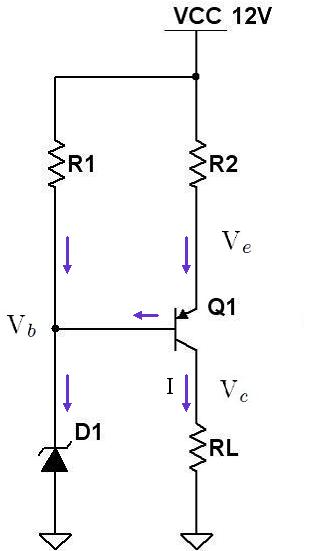
In theory, at Any load higher than 500 ohms will get less current, until eventually the collector junction will remain open and no current will flow (except a maybe a few picoamps from any leakage currents of the transistor). But this is not happening. I tried resistances above 500 ohms and the voltage continues growing.

Can you understand why?

Thanks!
 

First, you added the required resistor, but didn't make the other required changes. You need to take the voltage for R1 and R9 from the cathode of the zener(which is 9V). Your circuit is still using 10V as a reference.

As for your constant current source simulation: you've got a nominal 9ma current source (5.1v+.7v)/680. Then you put a 10K ohm resistor in the current path: 10K*9ma==>93V!!! Of course you're way outside the usable load range for this CCS. You have to determine the maximum resistance you want to measure, and then pick your current accordingly so that you don't saturate your transistor. For your circuit, the most voltage you can have across the load is about 6 volts==> 6/.009=>666 which is the maximum allowable resistance.
 
Barry:
Great! It seems that we are getting close! :-D

The PROPOSAL_2 provides an output range +0.5 to +9.5V with the R_DUT referenced to ground and using +10V:


The only issue now is that it has still a non-linear transfer function; so now I will focus in make it linear replacing R1 by a Current_Source.

But coming back to my question regarding the Current_Source example, I have open 2 questions:


a) What will happen in the REAL_WORLD (not SIMULATIONS) if the R_DUT goes above 666 Ohms? (Will it break the PNP Q1 transistor? or Does it simply will not conduct as I understood? :shock:
b) Why in my simulation can I increase the R_DUT above 666Ohms and the transistor continues turned ON and the voltage across R_DUT continues increasing above +5V? :???:

Thanks!
 

The only issue now is that it has still a non-linear transfer function; so now I will focus in make it linear replacing R1 by a Current_Source.
Did you undertstand, that the linear transfer function implies a resistance range of 0 to 23.3 kohm (if 11 kohm is set to 4.75 V)?
 
FvM:
What do you mean? Maybe that my R1 must go from R1=0...23K3?
 

Not R1. R_DUT can be measured between 0 and 23.3, but not above this value.
 

OK, I will substitute R1+R_DUT from PROPOSAL_2 with the Current_Source subcircuit and I will post a screenshot with the full circuit:

"PROPOSAL_2 + Current_Source"

I will keep you updated guys! Thanks! :roll:
 

Barry:

a) What will happen in the REAL_WORLD (not SIMULATIONS) if the R_DUT goes above 666 Ohms? (Will it break the PNP Q1 transistor? or Does it simply will not conduct as I understood? :shock:
b) Why in my simulation can I increase the R_DUT above 666Ohms and the transistor continues turned ON and the voltage across R_DUT continues increasing above +5V? :???:

Thanks!

Once R_dut exceeds 666, the CCS no longer provides CONSTANT current; the voltage will rise, but it will no longer be linear with respect to resistance as the transistor goes into saturation. If you need to measure higher resistances, you need to lower the current (by raising the value of R4. e.g.)

You won't 'break' the transistor. In your simulation you should be able to see the value of current through R5 is constant over a range of about zero to 666 ohms, and then it will decrease above that resistance.
 
To fulfill the voltage range specification, the current source needs to supply full output current up to 9.5 volt. The suggested circuit obviously doesn't. Also the current has to be reduced to about 0.39 mA. You'll face difficulties to implement the voltage range with 12V supply. A possible workaround is to increase the differential amplifier gain and adjust the constant current respectively.

For load and temperature independent current, I would refer to an OP current source.
 

Barry:
Thanks a lot!, I am trying the proposals; I will post a screenshoot. ;-)

FvM:
Thanks a lot by the new suggestion!; but what do you mean with "OP current source"? Could you provide me with an example (maybe a weblink) to clarify, please? :-|
 

I have added the Current Source in PROPOSAL_2:


But I don't achieve the expected output range from +0.5V to +9.5V if R_DUT=0...11KOhm.

I tried to different implementations:

a) Implementation A:


b) Implementation B:


Could you take a look and see what can I change? :-| (I think that adding the Current_Source sub-circuit, I have to follow the Implementation_B and ignore the Zener from Proposal_2; keeping only the Zener from the Current Source; but I am not fully sure :sad:)
 

Looking (briefly) at implementation A. The current from the CCS is about .2/375=0.53mA (assuming Vbe=0.6V). 0.53mA x 10K==>5.33V. The transfer function of the output stage is: Vout =V(U4out)+V(U5out). So, you should expect to see about 5.8V on the output. Is that what you're seeing?

Looking at implementation B, you're right, you don't need the zener if you're going to use the CCS, but you DO need to change that 590 resistor to give you 0.5V out of the bottom opamp.

However, I think you're probably going to need a more accurate CCS (as mentioned before by FvM). There's too much variation in the BJT parameters to make this usable over a wide resistance range.
 

Barry:
Then, I will continue working only with Implementation_B because is simpler ;-). But two questions about it:

1) Why do I need to change the 590 resistor? I think that it is good for my +0.5V bottom range, isn't? :shock:
(Maybe is 536 Ohm value more accurate to achieve the bottom +0.5V? Did you mean that? :-| )

2) Why do I need a more accurate CCS? Which do you think that could be the maximum R_DUT range from "0 Ohm...X Ohm" for which the actual Implementation_B is still OK? :???:

3) Anyway, do you have any circuit example of a more accurate CCS? :roll:

Thanks!!!
 

1) Because you changed the reference for the top of your voltage divider from 9V to 10V!!! 590/(10000+590)*10=.557 volts, not .5V

2) Because the current from the CCS depends on the accuracy of your zener, Vbe, the hfe of the transistor (may vary from unit to unit), temperature effects, etc. A change of 10uA would cause an output change of 0.1V on the output with a 10K resistor. Is that acceptable for your application? You need to establish some requirements first, and then go from there.

3) There are a lot of ways to get more accurate current sources. For starters, use a bandgap reference (instead of a zener). Use an opamp circuit. Look on the web, there's lots of stuff out there.
 
Barry:
1) OK, I changed to 536 Ohm.
2) OK, I will check.
3) OK, I will take a look.

Thanks!
 

Status
Not open for further replies.

Similar threads

Part and Inventory Search

Welcome to EDABoard.com

Sponsor

Back
Top