Continue to Site

Welcome to EDAboard.com

Welcome to our site! EDAboard.com is an international Electronics Discussion Forum focused on EDA software, circuits, schematics, books, theory, papers, asic, pld, 8051, DSP, Network, RF, Analog Design, PCB, Service Manuals... and a whole lot more! To participate you need to register. Registration is free. Click here to register now.

How to clip (define) the output signal?

Status
Not open for further replies.

torakaru

Member level 2
Joined
Apr 4, 2006
Messages
48
Helped
3
Reputation
6
Reaction score
3
Trophy points
1,288
Activity points
1,662
How to clip (defined range) the output signal of an In-Amp?

Hello Folks,

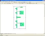
I have designed a circuit (basically an Instrumentation amplifier with G=1, with 3 single OpAmps), to measure the differences in resistance, when I place a resistance in their inputs that can go from zero (shortcircuit) up to infinitum (open-circuit) ohms:


So, depending of the value of the "R_for_Test", the output of the OpAmp U1 will go from 0V up to +10V approximately.

Well, my question comes now. If I would like that the output range of U1 will go ONLY from "+0.5V up to +9.5V", how would be possible to be done easily?

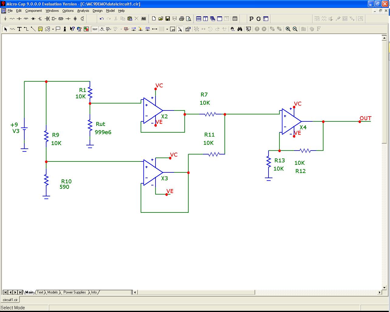
I though about the following solution (I added a resistor divider at test_pad_1):


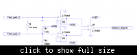
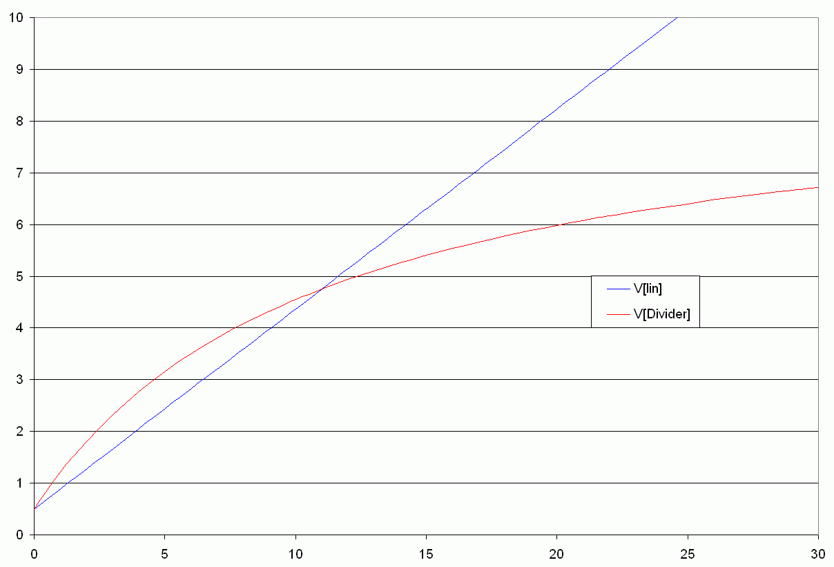
But the problem is that the output goes from "0V up to +9.5V", but not from "+0.5V up to +9.5V".

Do you have any idea to help me, please?

Anyway, thanks a lot in advance!
 
Last edited:

how about this (I'm not quite sure about inserting images...):
 

Attachments

  • schem1.jpg
    schem1.jpg
    97.4 KB · Views: 96
The shown circuit has several issues and can't work:
- GND connection of U2 +ve input is outside specified common mode range
- U1 misses the gain setting resistors of the typical instrumentation amplifier circuit. As shown, U1 will be continuously in pos. or neg. saturation
 
FvM is right. Further, you won't be able to drive the output lower than a volt or two above ground. You might want to look at a different opamp, or use split supplies.
 

Barry:
1) Thanks by your proposal (I am really using the Quad Opamp LM224, and NOT the LT1001);... but following your advice, if I want to achieve an output from "+0.5V up to +9.5V", which should be the values of the 4 resistors that you proposed me (R6,R7,R9,R10) if in my circuit I used one of 11KOhm? (How I calculate them?)

2) Should I chage LM224 by another Opamp to achieve the "+0.5V up to +9.5V"? Any recommendation to search it? :roll:

FvM:
1) Why you said that "GND connection of U2 positive input is outside specified common mode range"? (I tested the circuit with real components and it seems that it works for different values of "R_under_test" without any trouble, but from 0V up to +10V) What I missed? What I doing wrong? :shock:

2) You were right, U1 missed the gain setting resistors in that screenshot, but in my full circuit I have them (all four equal to 100KOhm); only I didn't draw them here to simplify the schematics.

Thanks again to both by your help! ;-)
 
Last edited:

Fvm spoke of the common mode limit because your schematic showed LT1001 not LM224. Calculate your resistors as follows: assume your test resistor is zero. The total voltage across r6&r7 should be 0.5. Then assume test resistor is infinite; the voltage on the top voltage divider should be 9.5v higher than the bottom one.

I'm not even sure this is solvable; I was just throwing it out there as a starting point. You might want to try simulating this with Microcap(free!) or similar program. Let me know if you still have problems calculating this.
 
I am really using the Quad Opamp LM224, and NOT the LT1001.
U1 missed the gain setting resistors in that screenshot, but in my full circuit I have them (all four equal to 100KOhm); only I didn't draw them here to simplify the schematics.

Amazing!

This two points caused the discussion to completely miss your initial question. Not surprizing, I think. You should really thinka about how to present a problem adequately. Obviously it's less effort to draw a correct circuit than to clarify all misunderstandings brought up by a "simplified" or simply incorrect one.

Now imaging your real circuit, there are some detail questions. I understand, that you want a clipper circuit. Yes this has been mentioned even in the title of your first post, but... (see above).
- What's the specification of the clipper? 0.5 V exactly or round about? Referring to the 9.5 V upper limit you reported as a feature of your circuit, this isn't more than a result of typical LM324 data without a guaranteed tolerance. So we have to ask for the accuracy requirements of 9.5 V limit as well.
- The LM324 (or any single supply OP) can't buffer the 0 V input voltage exactly, there's an error due to output saturation. What's the acceptable voltage error?
 
Barry
I have been simulating your proposal (I was using LTSPice IV because it is free also and very easy to use):


But I don't know how to calculate the 4 resistors to achieve the clipping that I want : +0.5V to +9.5V) :???: The best that I achieved are the values of the attached picture, but they give me a range in the output voltage of +0.5V to +9.9V; so it is not clipped at +9.5V

Could you help me to calculate the resistors that you suggested me to achieve the range +0.5V to +9.5V, please ?

FvM
Firstly, sorry if I confused you; you are right, I should drawn a more complete circuit from beginning, but for instance, LM224 is not available in the LTSpice IV and my teacher is pushing me to get a solution :-|

And regarding the specification of the clipper, I need +0V5 to +9V5, but "0.5V +/-0.1" to "9V5 +/-0.1V" would be also fine. I know that I will have some tolerances.

So, currently my "full detailed" circuit goes from 0V to +10V:


Do you have any suggestion to achieve the clipping range desired

Thanks a lot!
 
Last edited:

My circuit won't work. I need to rethink this. Sorry for the confusion.
 
OK Barry, I look to hear from you. Thanks a lot!
 

Ok, this should work. The 9v supply on the left side could be a zener, or some other kind of voltage reference. The output of X3 is simply a buffered 0.5V offset voltage. (You could also use a reference instead of the voltage divider). When Rut=open, 9V will appear on the output of X2, which is summed with the 0.5V offset to give an output of 9.5V at X4. When Rut=zero, the output of X2 is zero, and the output of X4 is 0.5V. Keep in mind that this is not a linear transfer function. (Vout=Rut/(R1+Rut)*9+.5) If you need a linear system, you could replace R1 with a constant current source(but that will limit the maximum resistance you can measure before the circuit clips; in other words, above a certain resistance the output will be constant).


Thanks Barry. Are you feeding the OpAmps with Vc=+12V? By the way, I must to implement a linear transfer function because I will use an ADC and MCU to capture and processing the output analog signal :-|; so, how could I implement your proposal of a "constant current source" to replace your R1?
 

I fear, I still don't understand the "clipper" specification. What has been shown yet isn't a clipper in my view. It's a circuit that presents a limited input signal to the amplifier and thus get a limited outpt signal. In my understanding, a clipper limits the output signals independent of the input. Please clarify. It usually involves diodes or utilizes output stage saturation.
 
Barry:
1) Thanks by your second idea, and while you reply to my question of the above post (your second proposal); I was playing a bit more with your first idea that you said that won't work:


Well, the point now is that I achieved the output range of "+0.5V up to +9.5V" thanks to the Zener (at least in simulation); but now I am not sure if my system has a linear transfer, or not. What do you think?

2) Secondly, I have simulated your Second proposal:


But the achieved output range goes from "+0.5V up to +10.5V" (So, it is still not good) But maybe I am doing something wrong? :???:

FvM:
Well, maybe I am using a bad terminology. So, forget the word "clipper" or "clipping", and think that what I need is a linear transfer output voltage which range is "+0.5V up to +9.5V" when I measure a "Resistor" and this resistor can have a value from "0 Ohm" up to "Infinite Ohm".
And although I implemented using 3 OpAmps, and I achieved initially a range of "0V up to +10V"; what I really need is to modify my initial circuit to achieve a linear output voltage range of "+0.5V up to +9.5V".

Is it clear now for you? Let me know, please :roll:

By the way, what do you think about the ideas that I am discussing with Barry?

Thanks a lot to both! ;-)
 
Last edited:

Thanks for clarifying. I would describe the operation as "adding a 0.5 V offset".

Do you need the resistor to be ground referenced (one terminal connected to ground), or can it be floating as well?

There have been two contradicting solutions discussed, and I'm not sure which one fulfills your intentions:
- Resistance 0 to infinity is converted into 0.5 to 9.5 V output. This implies a nonlinear resistance to voltage characteristic.
- Linear resistance to voltage conversion. This involves a certain resistance value, that is converted to 9.5 V. Resistances above this value will either give higher voltage or the output has limited artificially (clipped).
 
FvM:

Yes, I need the resistor to be ground referenced (one terminal connected to ground). [But, of course, if following that "design approach" is not possible to find a solution to make a defined "0.5 to 9.5" linear output; I would accept another suggestions ;-)]

But regarding your second question, I explain you what my teacher told me. My teacher told me that we will measure a resistance between the two testing points of my system. And for:

a) Short-circuit (so a resistance of 0 Ohms): The output signal must be +0.5V (and not bellow)
b) Open-circuit (so a resistance of infinitum Ohms): The output signal must be +9.5V (and not above)
c) 11K Ohms: The output signal must be around +4.75V (so this would be the middle point of the line)

And the system needs to be linear (from 0.5V to 9.5V) to make more easy the capture and processing using an ADC + Microcontroller; because the software involved will be more easy. (Even taking into account tolerances of components)

So, what I need is your second suggestion: "Linear resistance to voltage conversion. This involves a certain resistance value, that is converted to 9.5 V. Resistances above this value will either give higher voltage or the output has limited artificially (clipped)"

Then, what do you think about the circuits discussed until now? What will you recommend us?

Thanks!!!
 

As I think we all now understand this, you really don't want a clipper, and, as FvM said, you want a 0-9v span with a 0.5V offset. That's basically what I showed in my last schematic. Regarding your first simulation, that won't work because the output of U2 is going to always be 5V (assuming that's a 5V zener on the input). The second simulation is ALMOST what I showed, but you've go a problem there. I think you've got a 9V zener there, but it's connected right to the 10V supply. You need to put a resistor in series with the zener (and take your 9V off the cathode of the zener).

As far a using a current source, you need to establish the range of resistances you're going to be looking at; you can't have zero to infinity and expect a linear output-there has to be some upper limit.
 

Barry:

Sorry, but I don't fully understand you, so I will re-formulate, and we can refer to PROPOSAL_1 and PROPOSAL_2 circuits ;-):

1) If I simulate your PROPOSAL_1, (below screenshot) but with an added zener of 9,5V (BZX84C9V5L):


I achieved the output range of "+0.5V up to +9.5V" thanks to D1 Zener (at least in simulation); but now I am not sure if my system has a linear transfer output, or not. What do you think?

2) If I simulate your PROPOSAL_2, (below screenshot) but with an added zener D2 of 9,0V (BZX84C9V0L):


the simulated output range goes from "+0.5V up to +10.5V" (So, it is still not good). Is this fault due the missing extra series resistor that you requested me to add between V2 and D2? (But, Should I placed between V2 and D2, or between D2 and GND?)

But anyway, this PROPOSAL_2 is not linear, isn't? :sad: So, can you draw a circuit to make it linear taking into account what I explained to FvM, please?


Thanks! ;-)
 
Last edited:

Following the given specification, you can either have a linear R-to-V characteristic (involving a current source or a similar circuit), or a Rref to Rdut divider (resulting in zero to infinity range)
 
Working backwards, Proposal 2 should have a resistor between +10 and D2, that way the cathode of D2 will be at 9V and the maximum circuit output will be 9.5 instead of 10.5. But it will be non-linear.

For proposal 1 (which I don't think was my idea!) will also be non-linear because it is also a voltage divider. If you want to investigate constant-current sources, there's lots of information on the web. Here's just one example:

Simple Current Source
 
Status
Not open for further replies.

Similar threads

Part and Inventory Search

Welcome to EDABoard.com

Sponsor

Back
Top