Continue to Site
Follow along with the video below to see how to install our site as a web app on your home screen.
Note: This feature may not be available in some browsers.
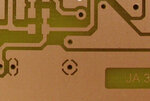
depends on your PCB manufacturer capability. in olden days 8/8 mil (width/ seperation) was common. But Now most of the manufacturers are capable for doing 4/4 mils but at a higher cost.
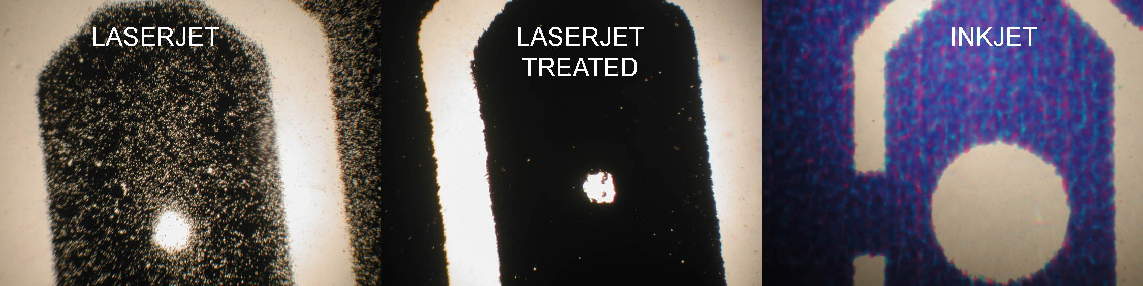
great advice in case we want to use laser jet...I did a brief study comparing inkjet to laserjet and to a modified laser jet transparency. The modification was simple. I took a Dry Erase pen and swabbed it across the laserjet transparency. After the ink dried, I wiped it off with soft tissue. The Dry Erase fills the tiny holes in the laserjet toner. If you try this, just apply the ink with a full, smooth stroke. Since you are removing excess later, cover the entire circuit image. DO NOT SCRUB the transparency with the marker, or you will remove some of the laser toner.