Continue to Site

Welcome to EDAboard.com

Welcome to our site! EDAboard.com is an international Electronics Discussion Forum focused on EDA software, circuits, schematics, books, theory, papers, asic, pld, 8051, DSP, Network, RF, Analog Design, PCB, Service Manuals... and a whole lot more! To participate you need to register. Registration is free. Click here to register now.

Questions of LM393 Comparator's application : Squarewave form generator

Status
Not open for further replies.

bhl777

Full Member level 6
Joined
Sep 30, 2008
Messages
363
Helped
0
Reputation
0
Reaction score
0
Trophy points
1,296
Activity points
5,140
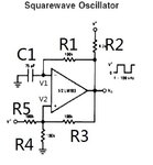
Hello everyone, this is a simple question of the application of square wave generator using LM393 comparator. I am still a little bit confuces of how it works.
(1)Could you have a look at the attachment to tell me the detailed analysis steps of it?
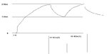
Since now I only know that V1 is a sawtooth wave and V2 is like a DC. But do not know how the feedback resistors work.
(2)At the mean time, could you tell me how to calculate the cycle of the output? Someone in the internet said it is like 1.1RC but I do not know how to figure it out.
Thank you so much!
 

Attachments

  • 1.jpg
    1.jpg
    40.5 KB · Views: 211

I can’t open the Wikipedia pages properly, so let us examine this specific circuit in a humble way.

It has 3 nodes other than V+ (we will refer to it as Vcc) and ground (assumed to be the reference node hence 0V).

At node V1 (IN-) we consider only the currents through C1 and R1 since the comparator input current is relatively very small (about 40nA).

At node V2 (IN+) we have therefore 3 resistors that determine its voltage.

As you know, the function of the comparator is to compare V1 and V2:
When V1 > V2 , the output voltage becomes low that is close to ground or 0V.
When V1 < V2 , the open collector output doesn’t sink any current.
The voltage difference could be a few mV only though its magnitude affects the response time; the greater the difference is, the shorter the time is.

You may say, but what happens if V1 = V2 (or they are very close). Unless there is a negative feedback, the comparator would have an undetermined state (due to noise perhaps) and this should be avoided as a permanent condition (though it always occurs during the input fast rising and falling edges). In fact, the resistor R3 is added here to avoid this fragile state (very high gain and very low input voltage). R3 forms a positive feedback, because it gives an input of the same polarity (direction) of the output.

Now it is time to do some calculations (from here the fun starts).
Fortunately this circuit has two alternating stable states only; when V1 > V2 and when V1 < V2.

When V1 > V2, hence Vo = 0 (actually close to 0):
V2 = Vcc * R3//R4 / (R5 + R3//R4)
Since R3=R4=R5
V2 = 1/3 * Vcc (nice result)
So in this state, C1 will discharge through R1 till its voltage (V1) reaches Vcc/3.

When V1 < V2, hence Io = 0:
V2 =[ Vcc/R5 + Vcc/(R2+R3)] * (R5//R4//(R3+R2))
Note: The small ‘varying’ current in R1 is neglected.
We usually go further and assume that R2 << R3 hence R3+R2 => R3.
V2 = 2/3 * Vcc
Yes, it is approximated to get another nice result ;)
In this state, C1 will charge through (R1+R2) till its voltage (V1) reaches 2Vcc/3.

If I remember well, a capacitor with an initial voltage Vc1 will charge through a resistor R to Vc2 toward a maximum voltage Vmax (as of a supply) by following the exponential time function:

Vc2-Vc1 = (Vmax-Vc1)*[1 – e^(-t/RC)]

In our case:
Vc2 = 2/3*Vcc
Vc1 = 1/3*Vcc
Vmax = Vcc
C=C1 and R=R1+R2

Therefore, the charging time (while Vo is high) is:
T_chg = RC * Ln(2) = 0.693 * C1 * (R1+R2)

The discharging function is rather similar and can be written based on above given data:
Vc1 = Vc2* e^(-t/RC)

Please note that the general formula is:
V_end – V_min = (V_initial – Vmin) * e^(-t/RC)

Here V_min = 0 , V_initial = Vc2 = 2/3*Vcc , V_end = Vc1 = 1/3*Vcc, C = C1 and R = R1

Therefore, the discharging time (while Vo is low) is:
T_dis = RC * Ln(2) = 0.693 * C1 * R1

For relatively high oscillation frequencies, the response delays should be taken into consideration.

I think this doesn’t answer your last question but please feel free to discuss anything you don’t see logical so far… I used to do always a few mistakes at exams :-?

Kerim
 
Last edited:
  • Like
Reactions: bhl777

    bhl777

    Points: 2
    Helpful Answer Positive Rating
Thank you KerimF, I have attached a picture of V- (which is named as V1 ) I drew according to the analysis method you taught me. Since at the very beginning, V1 should be 0, I drew it like that. Could you have a look at that to tell me if it is correct? (I think according to your analysis it is correct)
But I still have a question regarding you said about when V-=V+, the output will be in an undetermination state. If I do not use the feedback, just one input a DC level and other input a sawtooth waveform, the output will be a squarewave with a duty cycle. This is the principle of PWM. It does not require feedback, am I correct?
I can’t open the Wikipedia pages properly, so let us examine this specific circuit in a humble way.

It has 3 nodes other than V+ (we will refer to it as Vcc) and ground (assumed to be the reference node hence 0V).

At node V1 (IN-) we consider only the currents through C1 and R1 since the comparator input current is relatively very small (about 40nA).

At node V2 (IN+) we have therefore 3 resistors that determine its voltage.

As you know, the function of the comparator is to compare V1 and V2:
When V1 > V2 , the output voltage becomes low that is close to ground or 0V.
When V1 < V2 , the open collector output doesn’t sink any current.
The voltage difference could be a few mV only though its magnitude affects the response time; the greater the difference is, the shorter the time is.

You may say, but what happens if V1 = V2 (or they are very close). Unless there is a negative feedback, the comparator would have an undetermined state (due to noise perhaps) and this should be avoided as a permanent condition (though it always occurs during the input fast rising and falling edges). In fact, the resistor R3 is added here to avoid this fragile state (very high gain and very low input voltage). R3 forms a positive feedback, because it gives an input of the same polarity (direction) of the output.

Now it is time to do some calculations (from here the fun starts).
Fortunately this circuit has two alternating stable states only; when V1 > V2 and when V1 < V2.

When V1 > V2, hence Vo = 0 (actually close to 0):
V2 = Vcc * R3//R4 / (R5 + R3//R4)
Since R3=R4=R5
V2 = 1/3 * Vcc (nice result)
So in this state, C1 will discharge through R1 till its voltage (V1) reaches Vcc/3.

When V1 < V2, hence Io = 0:
V2 =[ Vcc/R5 + Vcc/(R2+R3)] * (R5//R4//(R3+R2))
Note: The small ‘varying’ current in R1 is neglected.
We usually go further and assume that R2 << R3 hence R3+R2 => R3.
V2 = 2/3 * Vcc
Yes, it is approximated to get another nice result ;)
In this state, C1 will charge through (R1+R2) till its voltage (V1) reaches 2Vcc/3.

If I remember well, a capacitor with an initial voltage Vc1 will charge through a resistor R to Vc2 toward a maximum voltage Vmax (as of a supply) by following the exponential time function:

Vc2-Vc1 = (Vmax-Vc1)*[1 – e^(-t/RC)]

In our case:
Vc2 = 2/3*Vcc
Vc1 = 1/3*Vcc
Vmax = Vcc
C=C1 and R=R1+R2

Therefore, the charging time (while Vo is high) is:
T_chg = RC * Ln(2) = 0.693 * C1 * (R1+R2)

The discharging function is rather similar and can be written based on above given data:
Vc1 = Vc2* e^(-t/RC)

Please note that the general formula is:
V_end – V_min = (V_initial – Vmin) * e^(-t/RC)

Here V_min = 0 , V_initial = Vc2 = 2/3*Vcc , V_end = Vc1 = 1/3*Vcc, C = C1 and R = R1

Therefore, the discharging time (while Vo is low) is:
T_dis = RC * Ln(2) = 0.693 * C1 * R1

For relatively high oscillation frequencies, the response delays should be taken into consideration.

I think this doesn’t answer your last question but please feel free to discuss anything you don’t see logical so far… I used to do always a few mistakes at exams :-?

Kerim
 

Attachments

  • 1.jpg
    1.jpg
    21 KB · Views: 96

Here is java simulation for relaxation oscillator.
See how current flow..............

Measure U, I an P real time values in points and components
Put cursor over wire or component

You can use scope and change component values.
Click right mouse button on joint points and over components.

Relaxation Oscillator

Regards KAK
 
Last edited:
  • Like
Reactions: bhl777

    bhl777

    Points: 2
    Helpful Answer Positive Rating
Thank you~
Here is java simulation for relaxation oscillator.
See how current flow..............

Measure U, I an P real time values in points and components
Put cursor over wire or component

You can use scope and change component values.
Click right mouse button on joint points and over components.

Relaxation Oscillator

Regards KAK
 

I have attached a picture of V- (which is named as V1 ) I drew according to the analysis method you taught me. Since at the very beginning, V1 should be 0, I drew it like that. Could you have a look at that to tell me if it is correct? (I think according to your analysis it is correct)?

You did well.
And as you already noticed, at the start Vc1 = 0 (not Vcc/3).
Could you deduce the initial charging time for this circuit?

But I still have a question regarding you said about when V-=V+, the output will be in an undetermined state. If I do not use the feedback, just one input a DC level and other input a sawtooth waveform, the output will be a squarewave with a duty cycle. This is the principle of PWM. It does not require feedback, am I correct

Usually the frequency of the sawtooth waveform is not very slow. Therefore the comparator output has no time to respond randomly during the very short time when V1 is close to V2. But in case we like to generate a PWM output for a relatively very slow ramp at the input, we usually add a small positive feedback (high resistance) just enough to cancel the effect of noise by giving a push to V2 to increase the difference.
 
  • Like
Reactions: bhl777

    bhl777

    Points: 2
    Helpful Answer Positive Rating
Thank you KerimF, yes the initial charging time is RCln3 when it goes from 0 to 2/3Vcc.

Could you please give me a picture to see how this positive feedback works for PWM generator? I appreciate that very much!
You did well.
And as you already noticed, at the start Vc1 = 0 (not Vcc/3).
Could you deduce the initial charging time for this circuit?


Usually the frequency of the sawtooth waveform is not very slow. Therefore the comparator output has no time to respond randomly during the very short time when V1 is close to V2. But in case we like to generate a PWM output for a relatively very slow ramp at the input, we usually add a small positive feedback (high resistance) just enough to cancel the effect of noise by giving a push to V2 to increase the difference.


---------- Post added at 19:10 ---------- Previous post was at 18:55 ----------

And I have a question of this circuit. It is a little bit different from what we talk about just now. Assume R1=R2, then the initial value of v+=VCC/2. If Vee=0, when V- charge to Vcc/2, output=0, then v+=0. Since the discharge of the capacitor will no longer goes to 0, which means V- will always be higher than v+, it will not be oscillator. But obviously I am wrong because this topology is used in a lot of place. Where is my wrong? Thank you!

**broken link removed**
You did well.
And as you already noticed, at the start Vc1 = 0 (not Vcc/3).
Could you deduce the initial charging time for this circuit?


Usually the frequency of the sawtooth waveform is not very slow. Therefore the comparator output has no time to respond randomly during the very short time when V1 is close to V2. But in case we like to generate a PWM output for a relatively very slow ramp at the input, we usually add a small positive feedback (high resistance) just enough to cancel the effect of noise by giving a push to V2 to increase the difference.
 

In case of PWM, if we have a jitter-free output (clean edges) there is no need for a positive feedback.
And if you like to discuss the case for which a positive feedback may be needed, please let me know the typical simple PWM stage you have in mind.

About the second circuit, are you sure that for this topology Vee could be made 0V and not a negative voltage (usually Vee=-Vcc though this not necessary for the oscillation to occur as long Vee is a negative voltage, preferably not close to zero).
For instance, we assume here that the opamp output is rail-to-rail type that is its upper/lower limits are close to its supplies.
 
Last edited:

Hi KERIMF, I will let know you about the pwm topology I have in mind. Could you also have a look at my another question above your reply:
"And I have a question of this circuit. It is a little bit different from what we talk about just now. Assume R1=R2, then the initial value of v+=VCC/2. If Vee=0, when V- charge to Vcc/2, output=0, then v+=0. Since the discharge of the capacitor will no longer goes to 0, which means V- will always be higher than v+, it will not be oscillator. But obviously I am wrong because this topology is used in a lot of place. Where is my wrong? Thank you!"
 

But obviously I am wrong because this topology is used in a lot of place.
There are more changes needed than setting Vee=0. Usually the voltage divider is biased to mid supply to get a symmetrical "triangular" waveform.

As an additional comment, the waveform is actually exponential rather than triangular. If you require a linear control voltage to duty cycle PWM characteristic, you would want to use an integrator based true triangular generator instead.
 

Status
Not open for further replies.

Similar threads

Part and Inventory Search

Welcome to EDABoard.com

Sponsor

Back
Top