Continue to Site

Welcome to EDAboard.com

Welcome to our site! EDAboard.com is an international Electronics Discussion Forum focused on EDA software, circuits, schematics, books, theory, papers, asic, pld, 8051, DSP, Network, RF, Analog Design, PCB, Service Manuals... and a whole lot more! To participate you need to register. Registration is free. Click here to register now.

bandGap reference PSRR question

Status
Not open for further replies.

!! the phoenix law !!

Member level 1
Joined
Nov 28, 2010
Messages
39
Helped
0
Reputation
0
Reaction score
0
Trophy points
1,286
Activity points
1,650
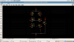
I have designed a BG reference which employs an opamp (typical BG)
my question is: How to enhance a BG PSRR ?
What are the factors that affect the whole PSRR ?
I am using a two stage OTA with miller compensation (I designed this before and just used it again to save time designing another single stage OTA for the BG)
The PSRR of my BG is -60db at DC, starts to degrade at 500Hz and reaches +15db at 10MHz, actually this is so bad for my application
I tried to replace the OTA with an ideal model, i.e: two vccs with an RC circuit at the output of each defining the BW, however the PSRR was -50db at DC degrades at 50MHz and never touches the zero
Also I tried to use the actual OTA but with another pure supply different than that one used for the mirror (which include vsin with vac=1 to simulate PSRR)
I obtained the same bad PSRR
!!!!!!!!!!!!!!!!!!!
Now i am very confused
1-Does the OTA affect the BG PSRR at all ? which parameters in the OTA have this effect ? the DC gain ? the BW ? should I design a single stage OTA instead of this two stage ?

2-I desgined the BG with 2v supply and 1.3v output (the vref), the current was also designed to be 1uA, Actually I tried to design for a 10uA but I couldn't get the expected curve vs temperature (the bell), also calculations show that vref can not be less than 1.2v to obtain the bell curve
Is this true ? which from the above stated parameters do affect the BG PSRR ?

Note: the BG is stable

Thanks Guys
 
Last edited:

Miller caps can completely degrade your PSRR depending on the feedback scheme used: if you have IEEE access look this up
"PSRR Improvement Technique for Amplifiers with Miller Capacitor"
Mikko Loikkanen and Juha Kostamovaara

In your case though you are seeing the problem even with an ideal supply on the OTA, right? How are you defining PSRR, I am guessing vref(AC)/vdd(AC), right? which is more aptly called power supply sensitivity while the PSRR is somewhat different being the ratio of the AC terms contributed at the output by supply and by the input acting separately, in particular with the OTA input at DC when you are measuring the contribution from the supply. PSRR is close to the inverse of supply sensitivity when operating in a unit gain configuration (hardly your case I imagine)

In any case having high loop gain helps reducing vout(AC) from both contributors so you want to keep the GBW as large as possible (unlikely in your application) but you also want to avoid a perfect single pole behavior, instead try to get the gain to flatten once you have decent gain margin below 0dB

Can you post your loop gain and PSRR plot?
 
Last edited:
The easiest thing is to feed it from a "poor man's LDO" if
you have the headroom for it. An NMOS source follower
with a lot of gate shunt capacitance to ground will take
out a lot of the HF AC. DC-Bias it with a VGS stack and
resistor. The downside is a fairly poor tempco of internal
supply.

Try a sensitivity analysis of sorts. Put a separate AC source
in each VDD-connected component leg and shotgun it. The
biggest responses want further looking. You may want to
depend whole current mirror racks from a single source
where you believe mismatched VDD activity would have
superlinear effect.

VDD-referred current mirrors are the easiest way to
get bad HF PSRR. The AC coupling to VSS adds to the
DC current. Cascoding the bias input with a VDD-gate
NMOS can help. At the cost of headroom again.
 
!! the phoenix law !! ,
Low-frequency bandgap's PSRR depends on OpAmp gain, but high-frequency one's doesn't. You can easily improve PSRR of your bandgap at high frequency by adding decoupling cap to Vref output. Try it.

dgnani,
I guess that for bandgap case PSRR definition as vref(AC)/vdd(AC) is correct.
 
Thx Guys,

@IADanilov
Adding a decouplig capacitor really improved the PSRR, simple and efficient
Thanks soooo much

Now, I have a question, how to size the BG mirror to optimize the TC ?
I am using 0.13 tech, can you suggest a value for both L and W ?

And How to optimize the TC in general ?

I have chosen n=8 for matching, the bias current is 1uA (R1=110k) to reduce consumption and enhance PSRR, By calculations I found that R2 should equal 645k (after a little simulation tweaking)
however I have arbitrarily sized the Tr's
The reultant curve is attached (vref around 1.3)

Is there any thing i am doing wrong ?
I need the difference between maximum and minimum vref to be 1m at most, how ? TC.png
 
Last edited:

Sorry Guys, I have another urgent question
I have designed a folded cascode OTA and used it in this BG
But Ibias was set as an ideal current source, the last step to complete the BG design was to replace this ideal source with another actual one, When i did so, both the TC and PSRR were very badly affected !!!
What should I do ?
The current source i am using is attached, is there another circuit should I use to solve this problem ?
Thanks
 

Attachments

  • Screenshot-1.png
    Screenshot-1.png
    51 KB · Views: 162

!! the phoenix law !! ,
I guess that sizes of mirror are based on parameters of your 0.13 tech and particular for every design. Do parametric analysis to choose appropriate sizes.

I think your resistors are too large (their die area go too far). If the goal of your design is to greatly reduce power consumption and die area doesn't matter, it's ok, but otherwise you should optimize resistor sizes to save area. For example, in my 0.18 process bandgap design (also opamp included) overall current consumption is about 80 uA, resistors are 3.5k and 11.75k and area is (110 x 85) um^2.

>I need the difference between maximum and minimum vref to be 1m at most, how?
I suppose that you never reach 1 mV difference between maximum and minimum vref with typical bandgap reference in practice.

>When i did so, both the TC and PSRR were very badly affected !!!
Could you show figures of TC and PSRR?
 

Hi phoenix,

1) Regarding your first question. There is not anything wrong with the curvature of your output. It is completely normal to expect variation of the output voltage around 2 mV. There is only first-order temperature compensation.
2) How to size the mirror? Probably you are doing right. You need to think guarantee that theses transistors does not go out of saturation in the corner cases. So you have the current, you have an idea of VDS, so you can estimate the proper W/L.
3) Regarding your current source. I guess something is wrong with your simulations. I have used this current source and it does not damage the BGR performance. It is only responsible to bias the amplifier. If the current changes a little bit with the temperature, your gain can change a little bit. But if you have an high open-loop gain, this impact is totally negligible.

Best regards,
 

If the headroom is enough, two cascoded Bandgap will improve PSRR greatly.
 
Status
Not open for further replies.

Part and Inventory Search

Welcome to EDABoard.com

Sponsor

Back
Top