Continue to Site

Welcome to EDAboard.com

Welcome to our site! EDAboard.com is an international Electronics Discussion Forum focused on EDA software, circuits, schematics, books, theory, papers, asic, pld, 8051, DSP, Network, RF, Analog Design, PCB, Service Manuals... and a whole lot more! To participate you need to register. Registration is free. Click here to register now.

How to define substrate layers in ADS momentum !!

Status
Not open for further replies.

kashan

Junior Member level 2
Joined
Nov 15, 2006
Messages
20
Helped
2
Reputation
4
Reaction score
2
Trophy points
1,283
Activity points
1,409
Hi,

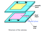
I have to design stacked patch antenna on ADS momentum. I know how to define single patch definition of substrate but i am not sure about my stacked patch. Attachment is my design which i want to implement in ADS momentum. I need to know how to define substrate layers for my particular stacked patch design.

Free space
Layer 1 = Parasitic patch
Layer 2 = Dieletric layer1
Layer 3 = Feed patch
Layer 4 = Dieletric layer2
Layer 5 = Ground Plane

Thanks in advnace and i am waiting for the reply.
 

Attachments

  • Stacked_Patch_final.png
    Stacked_Patch_final.png
    14.7 KB · Views: 370

Also i need to tilt plane 45 degree not the patch tilt to 45. Can anybody tell me how i can do this on momentum ?
 

Hi,

I have not used momentum for years now but i remember having similar issues at that time.
I solved the problem by loading substrate definition example of GaAs substrate for instance or PCB materials, in order to see how the layer where mapped. The documentation of momentum is also well done.

From what I remember, you have first to define the dielectric layers, and then in the next tab, you have to map metal layers in between the dielectric layers.
The layer 5 will be define as a close boundary if I'm right.
For the metal layers, you have to define if the geometry you need to draw is a slot or a strip. For a CPW line for instance, you can either choose to draw the center strip and the lateral ground planes strips or you can just draw the slot that will be substracted from a ground plane.
The most straightforward for beginners is to set all metal layers as strip.

Finally, in between metal layers, you can define via connections.

I hope it will help you !
reegards,
 
Thanks artiste. Your advice help me a lot. One more thing, can you tell me how can i draw the parasitic patch on the next dielectric layer? as i already draw the feed patch. Attachment is the snap for my design and results.

Also i want to tilt the plane 45° not the patch so how can i implement this ?

Thanks a lot.

 
Last edited by a moderator:

Hi Kashan,

to draw your parasitic Patch you have to assign (for example) your feed Patch on the "cond" metal layer and your parasitic Patch on the "cond2" metal layer. To do so you have to build teh following stack-up:

* Substrate Layers Tab:
FreeSpace
DielectricL2
DielectricL1
////////GND////////

then

* Metalization Layers Tab:
FreeSpace
----- cond2
DielectricL2
----- cond
DielectricL1
////////GND////////

cond and cond2 defined as "strip" for microstrip.

you won't be able to tilt the plane of your patch as Momentum is a 2.5D Solver. For this you have to get to a real 3D solver (CST, HFSS, IE3D, ...)

Hope it helps.

Cheers,

JB
 
I want to tilt the plane 45° in order to see the radiation pattern in azimuth plane. I do not have to tilt the patch array to 45°.
I am unable to find this option.

Hope u understood my point. Thanks a lot
 

Hope u understood my point.

Not exactly.

If you just analze "the normal way", you can plot far field for Theta = 0° to 90° and Phi = 0° to 360°.
I think this includes the data that you are looking for?

The only problem is that the substrates extend to infinity, which changes the result at the horizon.
 

Actually i want to analyze it on Theta = 0° to 90° and Phi = 45°. Thats y i want to tilt the plane. I am sending my radiation patterns design pictures. It will more clear the picture what i want. Hope it will help you to understand so that u suggest me some thing....


---------- Post added at 19:53 ---------- Previous post was at 19:50 ----------

Dear JB,

Can u have a look on my last post on this thread ? And suggest me what i will do in order to tilt the plane in ADS. I mean some other way to analyze the pattern in azimuth or 45 degree plane. Thannks
 

you can choose Phi angle in the 2D Settings from the radiation pattern window by choosing a planar cut angle of 45°. You'll then get a plot with Phi=45° and Theta varying from -90° up to 90° (see picture attached).
Hope I got your point

 
  • Like
Reactions: mwv101

    mwv101

    Points: 2
    Helpful Answer Positive Rating
Status
Not open for further replies.

Part and Inventory Search

Welcome to EDABoard.com

Sponsor

Back
Top