Continue to Site

Welcome to EDAboard.com

Welcome to our site! EDAboard.com is an international Electronics Discussion Forum focused on EDA software, circuits, schematics, books, theory, papers, asic, pld, 8051, DSP, Network, RF, Analog Design, PCB, Service Manuals... and a whole lot more! To participate you need to register. Registration is free. Click here to register now.

bandpass filter design using planar couple lines in ADS

Status
Not open for further replies.

atiqah3107

Newbie level 4
Joined
Mar 20, 2011
Messages
6
Helped
1
Reputation
2
Reaction score
1
Trophy points
1,283
Location
Malaysia
Activity points
1,325
hello all..
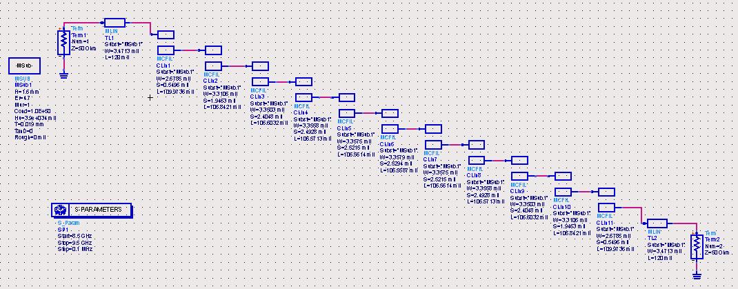
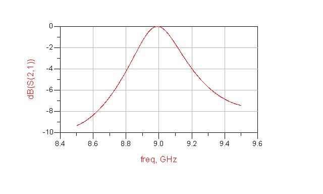
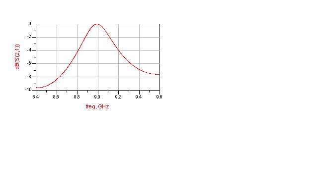
i have project a tittle "design bandpass filter design using planar couple lines" by using ADS software in 9GHz center frequency...but i still blur how to start design my project..can anyone help me....:roll:
 

hi....this is div patel....
in dsbsc modulation the bandpass filter is followed by balanced modulator.....to remove unwanted signals......
 

In ADS u have design guide template for BP ...
u can use that..

First of all, u need to know the specs of the filter.. insertion loss, return loss, rejection, cut off frequency, pass band ripple, BW..
 
tq for the reference...:)

this is my specification for my project....
Center Frequency, ωc 9 GHz
Upper Cut-off frequency 9.5 GHz
Lower Cut-off frequency 8.5 G Hz
Bandwidth 1 GHz
Insertion loss <30 dB
Chebyshev prototype 0.5 dB
Input and output port inpedance 50 ohm
Chebyshev Approximation


Before i find the order N for filter coefficients of Chebyshev filter, there are a few calculations are related, below is the related formulas are:
Bandpass transformation
ω= 1/∆ (ω_F/ω_o - ω_0/ω_F )
Normalized frequency
|ω|- 1=x
After know the order of N, we can refer to the table chebyshev filter with 0.5 dB ripple for N=1 to 10.
after calculation i get the order N is 10 for Fc 9Ghz..
did i'm do the right way to find the value of my design?...
someone please help...
 

hi
i attach an ADS tutorial for filter
 

Attachments

  • ADS filter Tutorial 2.pdf
    810.6 KB · Views: 198

i have try the design using ADS...this is the result...

the result for the graph is not the bandpass..how i want get the bandpass graph?...
 

1. I guess 5 sections maybe OK, if stop band is not OK, then increase sections. What is your stop band spec?
2. Between two line, there should be "step"
3. Set goals, let computer do it.
4. Consider errors, if your goal is 8.5~9.5GHz, then you should set say "8.4~9.6GHz".
 

at first i have set the start at 8.5GHz, stop at 9.5GHz and the step size is 0.1MHz...but the wave is look like at the above..
then i try change the the freq..start at 8.4GHz, stop at 9.6GHz and step size 0.1MHz...the result as below...


how i want get the real bandpass graph..did i make a mistake..i have follow the ADS tutorial step to design it....
 

The best thing would be use the template in the design guide (passive circuit control window)... in the schematic use DG-bandpass filter and then use ur passive circuit control window to control ur design... also u can set ur goals and optimize it accordingly..

Thanks
Venu
 

Status
Not open for further replies.

Part and Inventory Search

Welcome to EDABoard.com

Sponsor

Back
Top