Continue to Site

Welcome to EDAboard.com

Welcome to our site! EDAboard.com is an international Electronics Discussion Forum focused on EDA software, circuits, schematics, books, theory, papers, asic, pld, 8051, DSP, Network, RF, Analog Design, PCB, Service Manuals... and a whole lot more! To participate you need to register. Registration is free. Click here to register now.

[SOLVED] How to ensure correct symmetric component orientation?

Status
Not open for further replies.

bobsun

Full Member level 2
Joined
Mar 5, 2011
Messages
120
Helped
0
Reputation
0
Reaction score
0
Trophy points
1,296
Activity points
2,239
Hello,

I would like to ask a question on symmetric component orientation.

Most of the components are symmetric at least in one dimension, and most chips are square. For things like this, how can we ensure that they will be soldered in the correct orientation, when they are not soldered by machines out of tape and reel, but in prototyping by manual soldering?

symmetric orientation.png

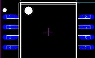
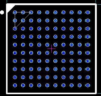
For example, the attached picture show a component whose pin arrangement is:
1 6
2 5
3 4

But after rotating \[{180}^{o}\] , they become
4 3
5 2
6 1

And if soldered in this way it will surely cause the system to disfunction.

So how could I prevent this from happening? Do I have to stand beside the solder worker and checking with component’s orientation from my laptop, and point out the right orientation?


Bob
 

Put a legend on the board that identifies the correct orientation, or provide an assembly drawing that shows it.

And train the assembly operator to do it correctly.
 
Last edited:
  • Like
Reactions: bobsun

    bobsun

    Points: 2
    Helpful Answer Positive Rating
Add pin1 marker on the PCB. inside & outside is better especially for prototyping.


The circle inside is the reference for the pin 1. The triangle outside is also a pin 1 marker which will be helpful in debugging if the component is already mounted.
 
  • Like
Reactions: bobsun

    bobsun

    Points: 2
    Helpful Answer Positive Rating
Add pin1 marker on the PCB. inside & outside is better especially for prototyping.

What is "inside & outside"? Do you mean putting the marker on both top and bottom layer?


Bob

---------- Post added at 09:26 ---------- Previous post was at 09:25 ----------

Mattylad,

Could you show an example?

Bob
 

What is "inside & outside"? Do you mean putting the marker on both top and bottom layer?

I placed an image on my last post. Circle marker is inside the component & Triangle marker is outside the component.

-KAK
 
  • Like
Reactions: bobsun

    bobsun

    Points: 2
    Helpful Answer Positive Rating
Dear KAK,

I see lots of blue and yellow crosses in your picture. Do they indicate power plane connection (different color for different planes)? I am using Altium Designer which also have such crosses so I would like to know if it is the same in your software.

And the silkscreen layer in your software is red?

Bob

---------- Post added at 09:48 ---------- Previous post was at 09:47 ----------

Dear NIKHILRAJ,

Great, I got it.

Bob
 

Dear KAK,

I see lots of blue and yellow crosses in your picture. Do they indicate power plane connection (different color for different planes)? I am using Altium Designer which also have such crosses so I would like to know if it is the same in your software.

And the silkscreen layer in your software is red?

Bob

Yes, you can set different color for different plane. Yes my silkscreen layer is red. Altium & PCAD is almost the same. its just that Altium is more capable on doing other things than PCAD. PCAD is a discontinued product from Altium.

-KAK
 
  • Like
Reactions: bobsun

    bobsun

    Points: 2
    Helpful Answer Positive Rating
Dear KAK, NIKHILRAJ and Mattylad,

What about for BGA components?

First, BGA components pins are not usually ordered as 1, 2..., but is alphanumerical combination like A1, A2...B1, B2..T1, T2..., so how do we mark?

And does BGA components (chips) have any indicator on them so they can be matched?


Bob
 

27_1300356085.jpg


Again pin1 marker inside & outside works for me. a small triangle on the edge for the inside & a large triangle outside.

Yes all BGA have a circle placed on the corner indicating the pin A1.

-KAK
 
  • Like
Reactions: bobsun

    bobsun

    Points: 2
    Helpful Answer Positive Rating
BGA ic have A1 indicator on it. You just need to put some marking in the silkscreen and assembly as in the case of SOIC.

IPC recommendation is a circle outside the componet and triangular chamfer inside


92_1300422188.jpg
 
  • Like
Reactions: bobsun

    bobsun

    Points: 2
    Helpful Answer Positive Rating
You have "an indication" of a polarisation of components.

Like you have a line at the end of a diode, or a + mark etc.

Whatever you come up with simply show your assemblers and train them to think smart, to understand how the components go.

Draw an assembly drawing to help them.

Give them nothing, tell them nothing and get back a PCB that is worth nothing (because it does not work).
 
  • Like
Reactions: bobsun

    bobsun

    Points: 2
    Helpful Answer Positive Rating
Dear KAK and NIKHILRAJ,

Many thanks for the attached picture. I fully understood it.

Bob
 

Status
Not open for further replies.

Part and Inventory Search

Welcome to EDABoard.com

Sponsor

Back
Top