Continue to Site

Welcome to EDAboard.com

Welcome to our site! EDAboard.com is an international Electronics Discussion Forum focused on EDA software, circuits, schematics, books, theory, papers, asic, pld, 8051, DSP, Network, RF, Analog Design, PCB, Service Manuals... and a whole lot more! To participate you need to register. Registration is free. Click here to register now.

[SOLVED] How could I control 50 Ohm impedance?

Status
Not open for further replies.

bobsun

Full Member level 2
Joined
Mar 5, 2011
Messages
120
Helped
0
Reputation
0
Reaction score
0
Trophy points
1,296
Activity points
2,239
Hi All,

I would like to ask some questions on impedance.

If I am having 5mil wide track, how should I do to control its impedance to 50 Ohm?

Because when I am referencing a design, it found its Gerber files has specification that all signal lines needs to be impedance controlled to 50 Ohm, however I found in the PCB file that


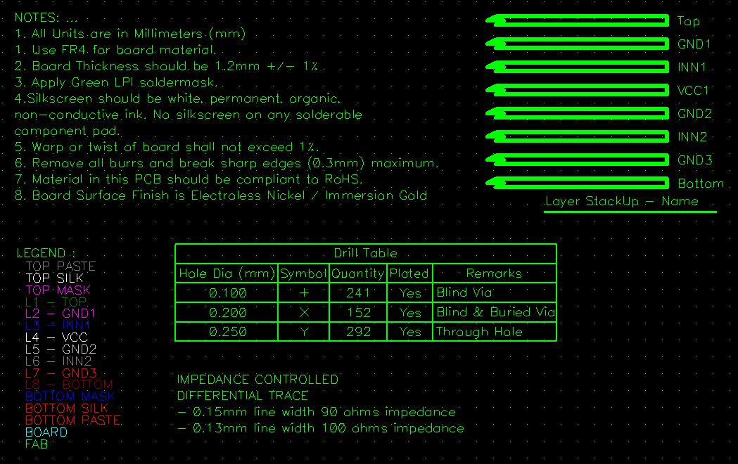
______________Material_______Thickness________Dielectric constant
Core__________FR-4__________12.6mil__________4.8
Prepreg_______ FR-4__________12.6mil__________4.8


layerstack.png

Using a impedance calculation formula

Z0=(K / sqrt (Er+1.41)) * Ln (5.98*h/(0.8*w + t))

\[{Z}_{0}= \frac{k}{\sqrt{Er+1.41 }}\cdot \frac{5.98h}{0.8w + t } \]

I took K=79 because 5<w<15 (87 if 15<w<25), and
1. Er=4.8
2. h=12.6
3. w=5
4. t=1.4mil

Due to the table above, which resulted in 83.56 Ohm impedance as calculated by the formula, which is much larger than 50 Ohm.

There are several parameters in the formula and the one thing I am sure about is that 5mil width needs to be ensured, but how about other parameters? Do I have control over h, and is it the same as prepreg thickness?


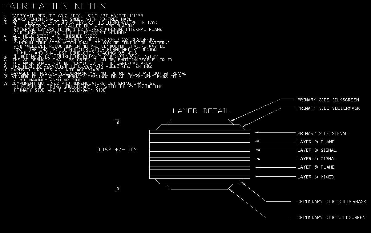
I have another question over how “h” is defined. If the signal trace is adjacent to a internal power plane, is “h” the thickness of the prepreg or core layer between them? If the signal trace is not adjacent to any power plane, for example, signal layers on layer 3, 4 and 5, and a power plane on layer 6, then how should I define h for trace on layer 4, which are two signal layers separated between power plane 6?

And is GND plane also included in the definition?


Thanks,
Bob
 
Last edited:

It is unusual to say, "I want a 5 mil trace to be 50 ohms." Unless you actually have a reason for fixing your trace width (i.e., fanning out from a tight BGA), the easiest way to obtain a controlled impedance line is by varying the width. The second parameter that can be varied is substrate. Different substrates have different dielectric constants, resulting in different impedances for a fixed width/height. Finally, you can vary height, although this is a little trickier, unless you are willing to pay high premiums to the fabrication house. Impedance controlled layers on external layers are actually a transmission line of type microstrip. For all intents and purposes, you must have a plane layer immediately below this layer (there are exceptions, but they come with severe restrictions). Internal impedance controlled layers are typically stripline, and have plane layers above and below them. You cannot have a reliable impedance controlled line on a signal layer surrounded by other signal layers. Planes used for impedance control may be either ground or voltage planes.

One typical way of conveying the desire for an impedance controlled line is to make all lines to be controlled a precise width (i.e., 5.7mils), and then putting a note in the fabrication drawing specifying that "all traces on layer 1 with width 5.7mils should be adjusted to be 50 ohms). Work with the board house early and often to ensure your requirements and design meet their capabilities.
 
I am fanning out from a tight BGA, exactly the case.

I would like to ask some further questions:

1. "Internal impedance controlled layers are typically stripline, and have plane layers above and below them." Does that mean I cannot have two signal layers next to each other, such as [plane - signal a - signla b - plane][? I think this is reasonable because when two signal layers are directly next to each other, there will be inductance between them, which could cause serious interference. Is that what you what is "severe restrictions" about?

But if all signal layers needs to be "sandwiched" by internal planes, then a consequence is that the layer stack must be arranged like:
layer 1 (top)
___plane 1
signal 2
___plane 2
signal..
___plane..
..
___plane k
layer k+1 (bottom)

and there will be a total of 2k+1, odd number layers. This is of course not the fact since all boards made from double-sided copper pads which after fabrication would always result in even number of layers. What is the mistake I have made here in the reasoning?


2. As far as I know the most common substrate material should be FR-4, which has Er typically between 4 and 4.5 So do you mean to use different substrate made from different material? Or, to vary h in the formula, which means to vary core/prepreg thickness. Is it possible?


3. Polygon pour

We have a classified transmission lines to two types here 1)microstrip, which is on top and bottom layers 2)stripline.

But when polygon pour (connecting to GND) is used on the external layers, can we still regard it as microstrip which has an immediate plane layer below it? Do we need to take the poured polygon, which is of considerable area, into consideration?

And if polygon pour is used for internal signal layers, does the “stripline” formula still valid?


Thanks,
Bob
 

Does that mean I cannot have two signal layers next to each other, such as [plane - signal a - signla b - plane][? I think this is reasonable because when two signal layers are directly next to each other, there will be inductance between them, which could cause serious interference. Is that what you what is "severe restrictions" about?

In 99% of cases, you must have planes on either side of an internal signal layer with impedance controlled lines. Furthermore, unless you want to greatly complicate your math, the dielectric thickness must be the same on either side of the layer in question. For external (microstrip) layers, it is not absolutely essential that there is a plane layer immediately below. However, it is highly recommended. Even if you have no traces on the second layer (the plane being on layer three), potential dielectric discontinuities between layers 2 and three could affect the desired impedance.

But if all signal layers needs to be "sandwiched" by internal planes, then a consequence is that the layer stack must be arranged like:
layer 1 (top)
___plane 1
signal 2
___plane 2
signal..
___plane..
..
___plane k
layer k+1 (bottom)

and there will be a total of 2k+1, odd number layers. This is of course not the fact since all boards made from double-sided copper pads which after fabrication would always result in even number of layers. What is the mistake I have made here in the reasoning?
It is unusual that all traces on a board are impedance controlled. Usually only extremely fast digital signals or analog signals have this requirement. For example, on an 1152 pin Xilinx Virtex 4, (hundreds and hundreds of i/o), a common design would only require the Rocket IO or LVDS pins to be impedance controlled. In that case, only one or two layers out of a potential 12 layer board would be impedance controlled (and need accompanying plane layers). Alternatively, you can always insert an extra plane layer to get the number of layers to an even number.

Example:

Layer 1: Signal
Layer 2: Plane
Layer 3: Signal
Layer 4: Plane
Layer 5: Signal
Layer 6: Plane
Layer 7: Plane
Layer 8: Signal
Layer 9: Plane
Layer 10: Signal
Layer 11: Plane
Layer 12: Signal

Are you sure that all of the "signal" traces in your design need to be impedance controlled?

2. As far as I know the most common substrate material should be FR-4, which has Er typically between 4 and 4.5 So do you mean to use different substrate made from different material? Or, to vary h in the formula, which means to vary core/prepreg thickness. Is it possible?


Yes, and yes. Other commonly used materials are Duroid, Rogers, and 370HR. Talk to your board house -- for the right amount of money, they will do just about any thickness (h) you want. However, if you work with them earlier in the design process, they can tell you what they normally stock -- and you can adjust your widths accordingly. This can significantly reduce fabrication costs.

3. Polygon pour

We have a classified transmission lines to two types here 1)microstrip, which is on top and bottom layers 2)stripline.

But when polygon pour (connecting to GND) is used on the external layers, can we still regard it as microstrip which has an immediate plane layer below it? Do we need to take the poured polygon, which is of considerable area, into consideration?

And if polygon pour is used for internal signal layers, does the “stripline” formula still valid?

Yes, the top layer is still microstrip. Depending on the frequencies involved, the distance from the edge of the trace to the polygon fill is usually pretty large. Typically, it does not need to be taken into consideration. Do you have a particular reason for flooding your external layers? As long as your 2nd and N-1 layers are full planes, you don't really need to be worried about EMI...

It is best to use unbroken planes in areas where transmission lines live. Discontinuities at plane boundaries result in nondesirable effects. Why would you flood internal signal layers with copper? I have not seen that done before, and it seems like that would increase the chances of a short somewhere internally on the board.
 
  • Like
Reactions: bobsun

    bobsun

    Points: 2
    Helpful Answer Positive Rating
Usually only extremely fast digital signals or analog signals have this requirement. For example, on an 1152 pin Xilinx Virtex 4, (hundreds and hundreds of i/o), a common design would only require the Rocket IO or LVDS pins to be impedance controlled. In that case, only one or two layers out of a potential 12 layer board would be impedance controlled (and need accompanying plane layers).
What about DDR2 interface? These lines spans four layers on the board I am referencing, so I think all these four layers needs to be impedance controlled?


Even if you have no traces on the second layer (the plane being on layer three), potential dielectric discontinuities between layers 2 and three could affect the desired impedance.
I didn't quite get what "second layer" "layer three" here refer to. There seems to be some ambiguity when referring to these layers. Does "second" layer mean the second signal layer, or the second physical layer? The same question applies to "layer three".

Shall we stipulate referring to layers like: T_phy_x, B_phy_x, Sig_x_Phy_x, Plane_x_Phy_x, GND_x_Phy_x?


It is best to use unbroken planes in areas where transmission lines live. Discontinuities at plane boundaries result in nondesirable effects.
Do you mean "split plane" by "broken planes"? I am using Altium Designer and it allows to cut internal planes to several regions, which they call "split plane"s. For example, GND plane could be cut to GND, GND_DAC, GND_ENC and so on, and power plane could be cut into VCC_3V3, 3V3_DAC and so on. And of course, these regions are separated by lines on which copper are removed. Do you mean that if transmission lines on adjacent signal planes cross (have their projection) these separations lines between different regions on a power plane, there might be nondesirable effects?

[qutoe]
Why would you flood internal signal layers with copper? I have not seen that done before, and it seems like that would increase the chances of a short somewhere internally on the board.
[/quote]
A board I am referring does that and I have no idea why they does.


Bob
 

I have not done a board with DDR. I would look at the data sheet for the chip in question and see what it recommends, rather than just trusting a reference design of questionable provenance.

The naming convention for layers I was using was strictly physical. I.e., "Layer 1" refers to the top, external layer, "Layer 2" the next physical layer, either plane or signal, etc.

Even in non-impedance controlled situations, split/broken planes are undesirable. The main reason is due to the lack of a "tight" return path for signals that are routed over the break. This results in larger current loops (more EMI), and more noise in your signals. These effects get compounded when the traces are treated as transmission lines. Unfortunately, due to the large number of voltages required on most modern boards, split planes are a necessary evil. There are white papers and books available on how to mitigate some of the effects of routing over a split plane for regular traces. I have never routed impedance controlled lines over a split between planes before, and do not know the actual effects beyond looking at the math. If possible, make your split plane shapes in a manner so that your signals do not need to cross a split.
 
  • Like
Reactions: bobsun

    bobsun

    Points: 2
    Helpful Answer Positive Rating
Dear hobbss,

According to your experience, does PCB designers usually put impedance control information in Gerber file as textual information, or specifies them when they are routing in the PCB editor? Which is more common?

I guess that is should be more natural for designers to make decisions on track width first in the designer, and only gets to specifying impedance control information later when they have exported the PCB file to Gerber file. Although they might already have read the data sheet and have the idea of how much impedance is needed for particular paths, in routing what they are primarily focusing about is the planar 2D layout, on things how can multiple tracks be routed out of a dense-pin BGA and so on. It seems to me naturally that they will defer impedance specification to the last phase.

So when we opened a PCB file, we might not need to take the track height, core/prepreg thickness, dielectric constant information seriously. They might actually be nothing but only the default values assigned by the particular EDA software (Altium, Allegro, etc.), having being ignored by its original designer in favor of specification in Gerber files, and are only typical values filled in by EDA software for most common tasks such as two-layer low-speed design.

Therefore, the only authentic information about material and impedance of a particular board, if that is obtainable, is the Gerber file. So if this reasoning and conclusion is true, then it solved my question in the first post of this thread that why I got different \[{Z}_{0 } \] from PCB and Gerber information: the PCB data are software's default information and are irrelevant.

What do you think about it?


Bob

---------- Post added at 22:53 ---------- Previous post was at 22:49 ----------

Dear hobbss,

Thanks for the additional answer on split plane. These are very important points and I will examine my board carefully to eliminate violation as possible.

Bob
 

Bob,

In defining the impedance of a certain line you first need to choose your board thickness depending on your application. If you're in to mobile application, board thickness is very important. From standard 1.6mm thickness, you can choose less than this on up to 1.0mm. Mobile PCB boards usually use 1.0 to 1.2mm board thickness. After choosing your board thickness you can use a stack up manager like POLAR and choose the desired thickness of every material in the stack up. Copper foil, core & pre-preg. a big effect on the line width is the gap between the copper foil & the plane layer next to it. Try using the common materials first & check the output line width for your 50ohms. When it is too thin or thick you can adjust the pre-preg so that it will match your needs. I also tried Altium for it's layer stackup but it doesn't give me good results that's why I shift to other stackup software. If you're routing DDR, you shouldn't pass any split plane, you can also see that on the layout recommendation on the chip you are using.

It is unusual to say, "I want a 5 mil trace to be 50 ohms."
+1 on this. normally you adjust the line width so that it will match your impedance requirement.

As far as I know the most common substrate material should be FR-4
Yes this is really common. I usually use this material.

I am fanning out from a tight BGA, exactly the case.
It is common that you use necking on the BGA and neglect its impedance requirement until it reaches the outside of the BGA.

According to your experience, does PCB designers usually put impedance control information in Gerber file as textual information, or specifies them when they are routing in the PCB editor?

This is in fabrication notes layer in gerber file

Hope this helps...

-KAK
 
  • Like
Reactions: bobsun

    bobsun

    Points: 2
    Helpful Answer Positive Rating
According to your experience, does PCB designers usually put impedance control information in Gerber file as textual information, or specifies them when they are routing in the PCB editor? Which is more common?

Both. Sort of. When impedance controlled lines are required, it is best to start thinking about them as early in the process as possible. If you haven't picked a board house yet, you can always do what I mentioned earlier -- use the constraint editor to force all lines that will be impedance controlled to be a strange width (i.e., 9.4 mils). Then you can work with the board house later by specifying, "All traces with width 9.4 mils shall be adjusted to be 50 ohms." By making the "strange" width large enough, you can ensure that there won't be proximity problems later when the board house comes back with their suggested width for the proposed stackup. At this level, the designer really needs to be thinking in 3D (including the stackup). Limiting yourself to 2D first, and worrying about the rest later usually just makes for more work.

So when we opened a PCB file, we might not need to take the track height, core/prepreg thickness, dielectric constant information seriously. They might actually be nothing but only the default values assigned by the particular EDA software (Altium, Allegro, etc.), having being ignored by its original designer in favor of specification in Gerber files, and are only typical values filled in by EDA software for most common tasks such as two-layer low-speed design.

This is somewhat true. I am sure the EDA designers give the values in these packages a lot of thought. However, it is always best to use the precise values received from your board house for these calculations. The equations are only as accurate as the values used in them. High end board houses know exactly what their dielectric constant is for any particular batch of substrate.


Therefore, the only authentic information about material and impedance of a particular board, if that is obtainable, is the Gerber file. So if this reasoning and conclusion is true, then it solved my question in the first post of this thread that why I got different \[{Z}_{0 } \] from PCB and Gerber information: the PCB data are software's default information and are irrelevant.

Personally, I typically create a Fabrication Drawing that has all of my precise specifications. My preferred format is .dxf. The post above has an example of some notes. The attachment here is another example. I have only included the notes and stack up section of the design. It would also include a board outline with holes marked and notated by a drill legend. Whether you put your notes in a gerber or in a separate drawing is up to you and the preferences of your board house. Whenever you send the board to the house for quotation, ensure that they receive the Fab drawing, acknowledge the specifications, and agree to them.

 
  • Like
Reactions: bobsun

    bobsun

    Points: 2
    Helpful Answer Positive Rating
If you have high speed tools such as a router and Signal Integrity tools you also require the stack information for these to work correctly, and if you are doing high speed design that requires controlled impedance it wont be long before you require these tools to take the guess work out of design.
 
  • Like
Reactions: bobsun

    bobsun

    Points: 2
    Helpful Answer Positive Rating
It is common that you use necking on the BGA and neglect its impedance requirement until it reaches the outside of the BGA.
When you use necking, can you still ensure that the tracks' characteristic impedance be the same everywhere within its length? It seems to me that necking is suitable only for non-critical low-speed signals. When the speed is high and if you use necking, how can you eliminate reflection?

When width narrows and impedance still needs to be the same, do you vary the height accordingly? If the finally processed copper foil is not of uniform height, how can it be put together with other layers, and how can it be matched with prepreg in-between? I guess it is mostly likely that necking is used only for low-speed non-critical signals, and when impedance control for high-speed signal is needed, necking should be avoid. Is it correct?

a big effect on the line width is the gap between the copper foil & the plane layer next to it.
Isn't the copper foil glued to the layer next to it? Where does the gap come from? Does it has anything to do with the thickness of the glue when it has cured?

---------- Post added at 17:45 ---------- Previous post was at 17:44 ----------

Dear KAK and hobbss,

I will study your attached files.

KAK:
What is your file format? Which software did you use to generate the file?

hobbss:
Is .dxf an AutoCAD format? Did you use AutoCAD to draw it or other software?


Bob

---------- Post added at 17:47 ---------- Previous post was at 17:45 ----------

If you have high speed tools such as a router and Signal Integrity tools you also require the stack information for these to work correctly, and if you are doing high speed design that requires controlled impedance it wont be long before you require these tools to take the guess work out of design.

What do your mean by "take the guess work out of design"?

Bob
 

Isn't the copper foil glued to the layer next to it? Where does the gap come from? Does it has anything to do with the thickness of the glue when it has cured?

He was referring to how thick the dielectric is, not really meaning the glue.


hobbss:
Is .dxf an AutoCAD format? Did you use AutoCAD to draw it or other software?

DXF is just a standard drawing file type. It can be opened with DXF viewers available online (freeware). I know Solidworks can open .dxf files, I have never used Autocad, so I don't know.

I create my fabrication drawings right in my EDA tool (Cadence flow), and export the data as a DXF file.
 
  • Like
Reactions: bobsun

    bobsun

    Points: 2
    Helpful Answer Positive Rating
I see these, thanks for the answer.

Bob

---------- Post added at 18:47 ---------- Previous post was at 18:42 ----------

hobbss and KAK,

hobbss said:
Furthermore, unless you want to greatly complicate your math, the dielectric thickness must be the same on either side of the layer in question.

KAK said:
after choosing your board thickness you can use a stack up manager like POLAR and choose the desired thickness of every material in the stack up. Copper foil, core & pre-preg.

hobbss suggest using symmetric plane thickness to not involve complicated math, but from KAK's description it seems that POLAR handles asymmetric case? Is POLAR's calculation accurate with asymmetric configuration?


Bob
 

Isn't the copper foil glued to the layer next to it? Where does the gap come from? Does it has anything to do with the thickness of the glue when it has cured?
Iit's the dielectric not the glue, just what hobbss said.

When you use necking, can you still ensure that the tracks' characteristic impedance be the same everywhere within its length? It seems to me that necking is suitable only for non-critical low-speed signals. When the speed is high and if you use necking, how can you eliminate reflection?
There are times that necking is inevitable. this is due to the pitch of the bga. that's why you need to limit the length of the thinner line width.

What is your file format? Which software did you use to generate the file?
I use gerber file. I'm using PCAD to generate the file.

hobbss suggest using symmetric plane thickness to not involve complicated math, but from KAK's description it seems that POLAR handles asymmetric case? Is POLAR's calculation accurate with asymmetric configuration?
symmetry is better. I never used assymmetrical in any of my designs. but POLAR can handle assymetric but I never tried that.
 
  • Like
Reactions: bobsun

    bobsun

    Points: 2
    Helpful Answer Positive Rating
The use of simulation software for high speed design is becoming not just a nice add on, but a necessity. A recent thread on DDR interfeces had a poll where nearly 99% reccomended or used simulation to check the layout for signal integrity. Doing a simulation on you high speed layout will confirm that the interface is going to work and there are no problems with the layout inb terms of signal integrity. If you dont simulate the high speed/fast rise time signals, then you can only hope that the layout will work as expected, afterr following reccomended practices. Thus using simulation/verification tools takes the guesswork out of the design, you can be certain the high speed layout will work as expected.
 
  • Like
Reactions: bobsun

    bobsun

    Points: 2
    Helpful Answer Positive Rating
I see them, thanks for the answer.

Bob

---------- Post added at 09:42 ---------- Previous post was at 09:26 ----------

Dear marce,

May I request the source of the pool?

Which software do they use for simulation? SPICE? I heard that SPICE is for circuit simulation only, so is it also capable of simulating high-speed signal, or high-speed signal are simulated using other software?


Bob
 

Status
Not open for further replies.

Part and Inventory Search

Welcome to EDABoard.com

Sponsor

Back
Top