Darkcrusher
Member level 5
Hi,
I've etched some EM loops:
The key is that performance depends on the etch angle. I'm therefore searching a good PCB supplier which can almost straight etch or mill or laser ?
Suggestions ?
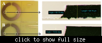
I've etched some EM loops:
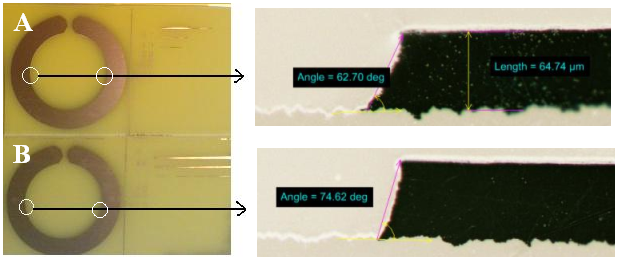
The key is that performance depends on the etch angle. I'm therefore searching a good PCB supplier which can almost straight etch or mill or laser ?
Suggestions ?