Welcome to our site! EDAboard.com is an international Electronics Discussion Forum focused on EDA software, circuits, schematics, books, theory, papers, asic, pld, 8051, DSP, Network, RF, Analog Design, PCB, Service Manuals... and a whole lot more! To participate you need to register. Registration is free. Click here to register now.
Can anyone say me how to design the layout of an nwell resistor of value 10K. I am trying to design the resistor in magic layout tool. please help..
thanks in advance
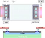
This is a simple well resistor under STI (Field), the cross section shows an NWell resistor.
For better isolation the resistor could sit in another well (for a triple well process). It could also be surrounded by an isolation ring and could have a metal field plate over the top of the resistor body.
This site uses cookies to help personalise content, tailor your experience and to keep you logged in if you register.
By continuing to use this site, you are consenting to our use of cookies.