kabaleevisu
Advanced Member level 2
- Joined
- Apr 14, 2010
- Messages
- 616
- Helped
- 85
- Reputation
- 170
- Reaction score
- 81
- Trophy points
- 1,308
- Location
- Chennai,India
- Activity points
- 4,512
Hi everyone,
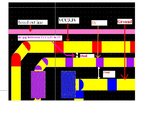
i designed xilinx usb jtag board, in this board nearly 120 via is present in the board if via affect design.i think this board should route in more than 2 layer ( in my design 3.3V ,1.8V,5V are used i think 4 layer is possible i doesnot know correct factor ) but in my client ask to design in 2layer i have dough via affect entire board
NOTE:
what are factor need to design high speed board (like 4 laye and 6 layer etc )to choose correct stackup
is it related to VCC and board size
because still now i am design 2 layer board only please any one help me to learn high speed design