Welcome to our site! EDAboard.com is an international Electronics Discussion Forum focused on EDA software, circuits, schematics, books, theory, papers, asic, pld, 8051, DSP, Network, RF, Analog Design, PCB, Service Manuals... and a whole lot more! To participate you need to register. Registration is free. Click here to register now.
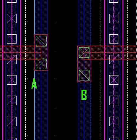
If you are "step-coverage challenged" then A is better
because the via sidewall step does not cut across the
current path (B, at least you have two parallel paths).
From the current density or current-per-via viewpoint - either design A or B may be better, depending on the pattern of the current flow.
For example, if the current flowing from M2 to M1 is split equally into two branches - then design A is better, as each via will be carrying one half of the total current in design A, while in design B the current in the upper (in Y direction or X-Y coordinate system of the GDS layout) via will be mush larger than in the lower via.
If the whole current in M1 is flowing up (in Y direction) - then design A and B are equally good (or bad) - as the whole current will be flowing through one (upper) via.
If the whole current in M1 is flowing down (in Y direction), then design B is better as the current will be distributed between the two vias, while in design A it will be flowing through one (lower) via.
It's very instructive to run a few simulations for current flow in interconnects like this - to quickly gain a physical insight into the current flow patterns, and get a better intuition. Then next time you do not need even to run any simulations - you will know what the optimal layout is, depending on the expected patterns of current flow.
there is one point that from current view, A is mostly better(2>1 situation as you descript, I am inclined to agree with you), another point that from lithography view, B is better, because A has 2 MT2 cross corner which B has only 1
---------- Post added at 07:10 ---------- Previous post was at 07:08 ----------
If you are "step-coverage challenged" then A is better
because the via sidewall step does not cut across the
current path (B, at least you have two parallel paths).
If you are "step-coverage challenged" then A is better
because the via sidewall step does not cut across the current path (B, at least you have two parallel paths).
Metal coverage (thickness) over the (more or less) vertical via wall areas usually is less than over the horizontal wires, at least for one side wall of a via, due to a possible shadowing effect if sputtering doesn't occur absolutely perpendicular to the silicon surface, see e.g. these SEM pictures. So if the current has to flow over such a lowly (if ever) covered via side wall, this presents a certain risk for either increased track resistance - if not an interruption.
This site uses cookies to help personalise content, tailor your experience and to keep you logged in if you register.
By continuing to use this site, you are consenting to our use of cookies.