Continue to Site

Welcome to EDAboard.com

Welcome to our site! EDAboard.com is an international Electronics Discussion Forum focused on EDA software, circuits, schematics, books, theory, papers, asic, pld, 8051, DSP, Network, RF, Analog Design, PCB, Service Manuals... and a whole lot more! To participate you need to register. Registration is free. Click here to register now.

Gm-C Integrator design...........

Status
Not open for further replies.

samiurrehman

Member level 2
Joined
Aug 30, 2010
Messages
49
Helped
2
Reputation
4
Reaction score
2
Trophy points
1,288
Location
Pakistan
Activity points
1,729
Dear all,

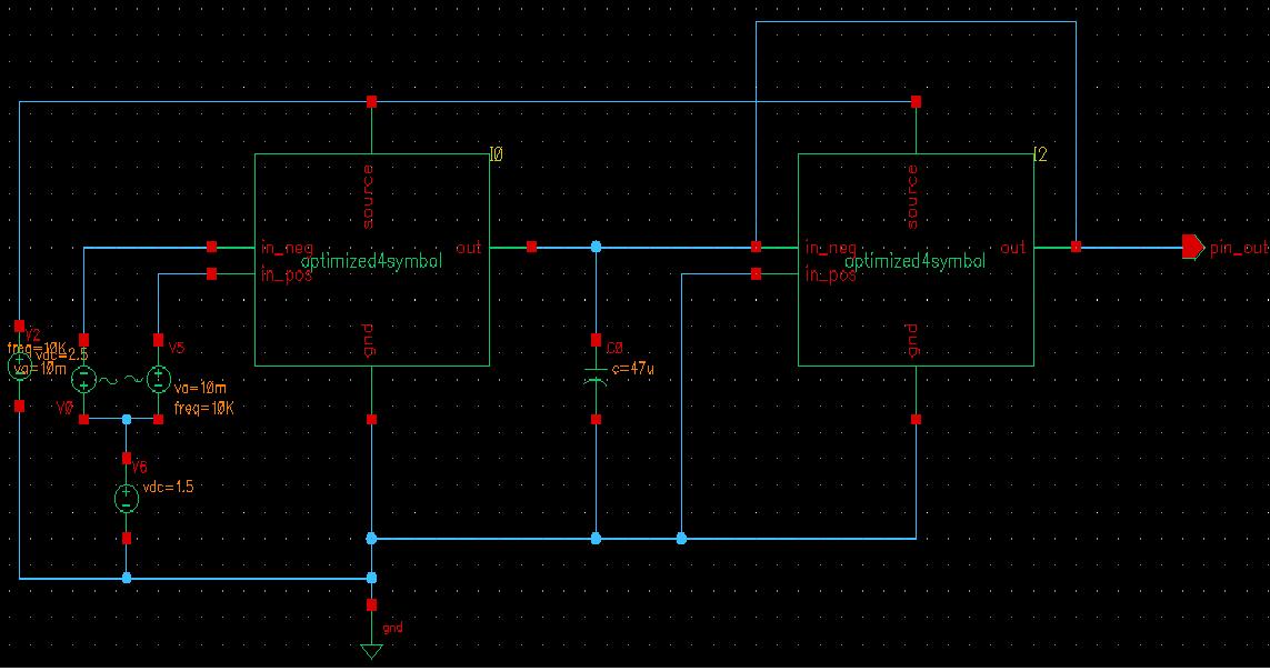
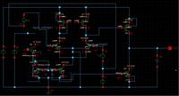
I have been asked to design Gm-C continuous time integrator with no rigid specifications. I have used a two stage OTA with 46dB gain and applied a capacitor at the end as integrating element. But the circuit is merely acting as an amplifier and not integrator. It does not convert square wave into triangular..... What modifications do i need to bring? Circuit schematic attached....


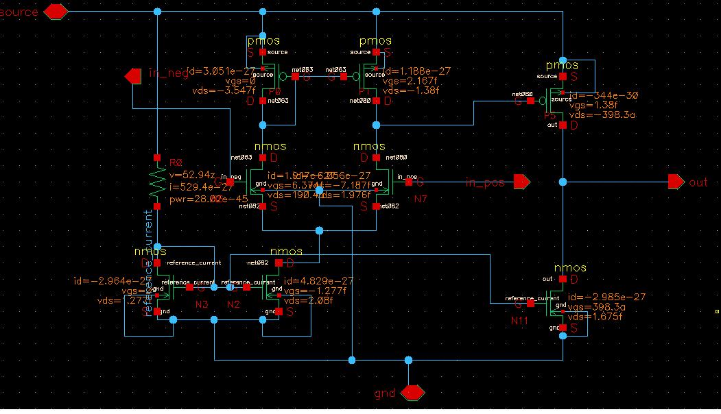
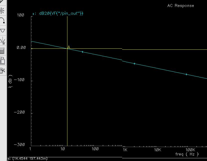
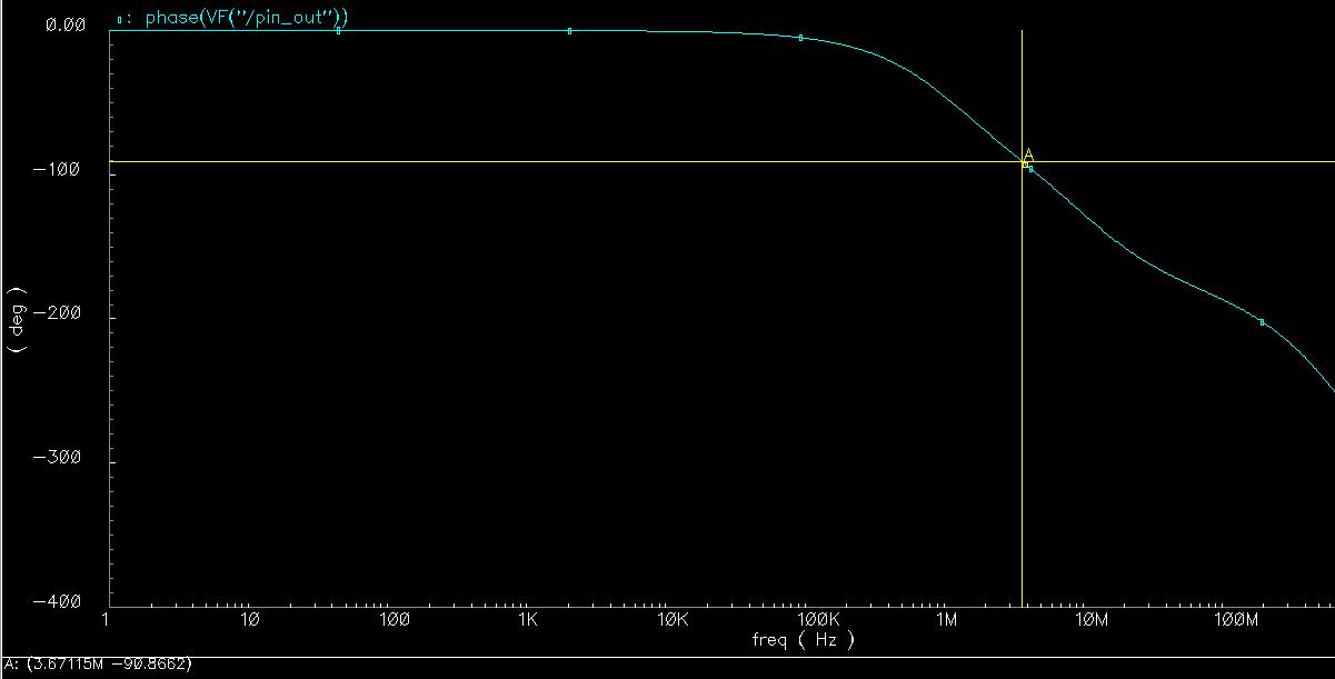
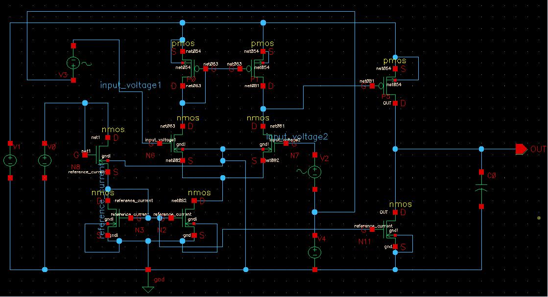
the circuit quite well acts as a low pass filter after installation of capacitor at the end...I believe just a capacitor at the end cant transform an amplifier into integrator......
 
Last edited:

... the circuit quite well acts as a low pass filter after installation of capacitor at the end...
I believe just a capacitor at the end can't transform an amplifier into integrator......
Very true: you have to use the capacitor as feedback element (to the negative input).
 

Part of the problem is that the configuration is open loop. Your amp has a high gain and most probably any signal at the input leads it to saturate. If you bias it correctly (i.e. apply the correct offset at the input so that the amp is in its linear region) and apply a very small signal it should work, but again, that is not practical at all. Therefore, you need a gm in a closed-loop configuration (e.g. putting the capacitor in the feedback loop as erikl suggested or putting the gm in unity gain feedback).
I assume you have checked that you are not using a too fast an input signal for your time constants?
 

What you've done is OK so far. Try putting to the output one more transconductor with negative feedback. Then you'll have three elements: OTA (which acts as a V-I converter) + C (which is teh integrating element) + OTA - neagtive feedback (active resistance). Your integrator is then the active equivalent of a classical RC lowpass circuit.

Gm-C circuits are very well described by Schauman or Sansen & Laker

Can you plz provide me with some links or material by Schauman or Sansen & Laker........i cant find any....Thanks
 

... Sansen & Laker........

I've uploaded a band-pass filter made un by two first order sections: one low-pass filter ( that is teh first two OTAs) and one high-pas filter (that is the last two OTAs). The first-order sections are taken from Sansen-Laker (it's a quite old book, 1994, so i don't think you'll find any electronic version of it).

So, the first two OTAs make the integrator. First OTA is actually a voltage-to-current converter and the second is an active resistance.

This should work...
 

Dear all,

I appreciate the suggestions made above for the help i wanted but still there is one major problem i am facing, the integrator BW problem. I increased the gain of my OTA from 45dB to 75dB but still integrator's gain is only above 0dB for a minimal BW. Let me explain things pictorially, below is the image of complete integrator architecture:

Each block represent an OTA with the following image:

but the problem is with the BW of integrator.....which is ridiculously around 10Hz???????See the image below:


i need help increasing BW of the integrator....Cap i am using in image 2 is 47uF.........
 

OK, sorry...

It seems that something went wrong when uploading the file. So I do it once more...
 

Attachments

  • GmC_1st_order.pdf
    26.4 KB · Views: 164

Check your DC operating points. At the picture you give your OTA isn't biased properly (everything is off).
 

    V

    Points: 2
    Helpful Answer Positive Rating
Dear all,

... there is one major problem i am facing, the integrator BW problem. ....Cap i am using in image 2 is 47uF.........

Well, a capacitor of uF is MUCH MUCH to big for Gm-C circuits. Try using only pF caps if you design specifications allow this. A rule o thumb (and nothing scientific in this statement): the bigger the capacitor, the lower the BW.

On the other hand, you can (slightly) adjust the integrator gain and BW out of the OTA bias currents. This of course presuming that the OTAs are already designed for your specifications.
 

Yes Mr.Kgl...... everything seems off because i just gave the circuit and did not connect the source...this was just what lies inside the OTA box in figure one...i simulated it unknowingly...
 

Fair enough. Phoibus is right then. Think of it like this: The transfer function of your integrator is something like gm1*R/(1+jwRC) where R=1/gm2, with gm1, gm2 the small signal transconductances of the first and the second OTA respectively. If you put the numbers you ll get the transfer function you get from simulation.
To simplify it even more, if you had an ideal integrator gm/jwC, for C=47uF, f=10Hz, and gm=1mS you get an amplitude of 3.38, which is close to what you get.

To increase the integrator gain you need to increase gm1 or gm2 or decrease C.
 

Well, a capacitor of uF is MUCH MUCH to big for Gm-C circuits. Try using only pF caps if you design specifications allow this. A rule o thumb (and nothing scientific in this statement): the bigger the capacitor, the lower the BW.

On the other hand, you can (slightly) adjust the integrator gain and BW out of the OTA bias currents. This of course presuming that the OTAs are already designed for your specifications.

Dear Phoibus,
Sure i totally agree with your rule of thumb but you know i am talking about the integrator BW (the slope, in a LPF for example)....If i use cap with less value my integrator acts more like a LPF, to eliminate the LPF BW, i used a large cap that is why i am getting just a tappered slope as AC response which matches with ideal integrator response. But this integrating BW reduces with the LPF BW.....this BW goes down the same with LPF BW.....
Can you provide with some material on Gm-C circuits??

Regards
 
Last edited:

I would suggest that you post a picture where the operating point of the OTA is clearly visible in your intended mode of operation. I have a doubt that the diff pair of the first OTA is well biased. You have a two stage OTA without a feedback. The second stage of the 1st OTA is loaded by a diode connected OTA, but the diff pair still sees only a capacitive load. Unless you use a very basic level1 model for the transistors, chances are that the diff pair is not well behaved.
 

Dear Phoibus,
Sure i totally agree with your rule of thumb but you know i am talking about the integrator BW (the slope, in a LPF for example)....If i use cap with less value my integrator acts more like a LPF, to eliminate the LPF BW, i used a large cap that is why i am getting just a tappered slope as AC response which matches with ideal integrator response. But this integrating BW reduces with the LPF BW.....this BW goes down the same with LPF BW.....
Can you provide with some material on Gm-C circuits??

Regards
Again, your pole is gm2/C. By increasing C you don't make it behave like an ideal integrator, all you do is move the cut-off frequency lower, out of the range you are plotting. If you plot lower frequencies you will still see it. It will only be a quasi-ideal integrator for frequencies above the cut-off. To increase the gain at a certain frequency (or the "integrating BW" as you say!), you need to increase the dc gain of the LPF. See the comments on my previous post.
 

Hi samiurrehman,

Since I was absent for some weeks: Are your problems solved in the mean time?
Anyway, do NOT use a capacitor in the feedback path of an OTA (as recommended by some forum members). This does not work. There are only two basic solutions for an OTA integrator:
1.) OTA with a capacitive load (high output impedance requires an additional buffer amp)
2.) OTA followed by an inverting opamp that has capacitive feedback (preferred solution because the OTA output impedance has only minor influence).
 

Dear LvW,

The integrator i designed has some problems.....It's integrating BW is very small...Actually i am still confused as to what are the characteristics of an ideal integrator.....now how do i demonstrate that i have built a nice integrator...it does not convert pulse into triangular......but can operate at 2G Hz....its a Gm-C integrator........My integrator has to be used in "digital modulator" used in RF front end....research is still underway...

Regards

What does it mean " it does not convert pulse into triangular......but can operate at 2G Hz.
Does it operate as an integrator or not?
An integrator is characterized by the integrating time constant T=1/2*Pi*Fc with Fc=crossover frequency (gain=0 dB).
the bandwidth of an integrator is defined by the phase excursion around 90 deg. An ideal integrator has exactly 90 deg phase shift. A realistic integrator can achieve this value at one single frequency only and its "bandwidth" is defined by the amount of phase error (for example+/- 1 deg) around this ideal value.
 

Your defination of BW is still confusing..this is my phase plot ...At 90 degree frequency is 3.6MHz...so what would be my BW of integrator
 

I don't think that the definition is "confusing", rather your circuit does not work as an integrator !
What is an integrator (defined in the frequency domain)?
It is a circuit with a magnitude slope of -20 dB/dec and a corresponding phase shift of 90 deg. But that's the ideal case. As mentioned before, the phase for real circuits is only approximately in the range of 90 deg - and the "bandwidth" (I do not like this phrase at all for integrating circuits) can be defined as a frequency range in which the circuit meets this phase requirement with some errors that seem to be acceptable.
Thus, you should try to adjust/modify your circuit with the aim to get in the frequency range of interest a magnitude drop of app. -20 dB/dec equivalent to a phase of app. +/- 90 deg (inverting/non-inverting operation).
 

Status
Not open for further replies.

Part and Inventory Search

Welcome to EDABoard.com

Sponsor

Back
Top