Continue to Site

Welcome to EDAboard.com

Welcome to our site! EDAboard.com is an international Electronics Discussion Forum focused on EDA software, circuits, schematics, books, theory, papers, asic, pld, 8051, DSP, Network, RF, Analog Design, PCB, Service Manuals... and a whole lot more! To participate you need to register. Registration is free. Click here to register now.

What's the phenomenon of a transmission gate?

Status
Not open for further replies.

urian

Full Member level 3
Joined
Sep 3, 2009
Messages
154
Helped
10
Reputation
20
Reaction score
3
Trophy points
1,298
Activity points
2,500
HI
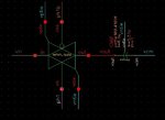
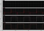
I have simulated a transmission gate,but the output plot as attactment contains some strange waveform.When the clock signal jumping high or low,the output will suddenly jump high and low,then return to the final value instantly.What cause these occur?Does it because the transmission will sorb electron as it begin to conduct and release electron when it begin to cutoff? Or because the clock feedthrough? Why the polarity looks like this?

Thanks for help
urian
 

Attachments

  • gate1.jpg
    gate1.jpg
    37 KB · Views: 133
  • gate2.jpg
    gate2.jpg
    117 KB · Views: 140

It is probably charge injection. You get signal coupled from the switching signals through the gate/source and gate/drain capacitance. Also you get channel charge storage.

Keith
 
  • Like
Reactions: urian

    urian

    Points: 2
    Helpful Answer Positive Rating
It's because you are using clock to control the transmission gate. The output will follow the clock though your input is constant.
 
  • Like
Reactions: urian

    urian

    Points: 2
    Helpful Answer Positive Rating
Thanks,
So the dominant is clock feedthrough from this plot?
 

It's not actually feedthrough but more towards controlling or gating using clock. That is when your clock is high your signal is allowed to pass through, when it is low, then it block your input signal, Vin.
 

The advantage of a simulation is, that you are able to visualize the voltage and current waveforms present at any single transistor in the transmission gate. You should look into this details, if you actually want to know the exact reasons for the observed behaviour, e.g. the feedthrough polarity.

More general, these are unavoidable properties of real world CMOS devices, introduced by varying and voltage dependand transistor capacitances, and the differences between N and P semiconductor materials. You'll find them in the specification of any analog switch.
 
  • Like
Reactions: urian

    urian

    Points: 2
    Helpful Answer Positive Rating
Status
Not open for further replies.

Part and Inventory Search

Welcome to EDABoard.com

Sponsor

Back
Top