Continue to Site

Welcome to EDAboard.com

Welcome to our site! EDAboard.com is an international Electronics Discussion Forum focused on EDA software, circuits, schematics, books, theory, papers, asic, pld, 8051, DSP, Network, RF, Analog Design, PCB, Service Manuals... and a whole lot more! To participate you need to register. Registration is free. Click here to register now.

LNA gain and input matching

Status
Not open for further replies.

yixiusky

Member level 2
Joined
May 8, 2008
Messages
46
Helped
0
Reputation
0
Reaction score
0
Trophy points
1,286
Location
Korea
Activity points
1,618
Hello everyone

I would like to ask one question

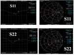
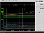
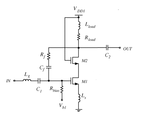
I designed one LNA works frome 1.8 to 2.2 GHz. After meausrement, the input and output matching are ok, but the gain shiift to 1.5GHz. I could not think the reason. Could you help me?

Thank you very much.
 

Layout design and component parasitics could be the reason of the frequency shift.
 
How did you measure input port?as we know inport is noise match,and not impedance conjugate matching.
 
Thank you very much every one.

I did more measurement, and i attach the result here.

(1) input matching S11 (both magnitude and smith chart)

(2) Output matching S22 (both magnitude and smith chart)

(3) Gain and NF

My LNA design is 1.8GHz to 2.2GHz, the peak gain should appear at 2 GHz.

However, the inputmaching peak is around 2GHz, but the output peak is at around 1.5GHz.

Then the peak Gain is also 1.5GHz. and the gain decrese around 5dB compare with post layer simulation result.

I do not know the reason why the Peak Gain is shifted to 1.5GHz, and also decreased around 5dB. Could you please help me? thank you so much
 

Attachments

  • summary.jpg
    summary.jpg
    203.2 KB · Views: 213
  • C1NF.GIF
    C1NF.GIF
    15 KB · Views: 207

i know typically measured gain is always lower than the post-layout simulation by 1~3dBs but i don't know if 5 dB is considered unusual? did you include the parasitic capacitors for post layout simulation? were your metal connections thick/wide enough? or does these result exclude the loss of the measurement cables?
 
i include the parasitic capacitors for post layout simulation. These results include the loss of the measurement cables. If exclude, the gain is around 13dB. But the peak gain still in 1.5GHz, shift from 2GHz.

my LNA is resistive feedback LNA.
 

Attachments

  • schematic.png
    schematic.png
    14.1 KB · Views: 201

You have increased VNA output amplitude level too much while you're measuring S11 therefore the measurements are not correct.The LNA goes into saturation.As a consequence the OP of the LNA might-probably-shifted somewhere because of autopolarization.
Decrease the output level of VNA and measure under low level signal condition..
 
When i measured my LNA, the signal power is low, around -40dBm. So i guess the output level of VNA has no problem.
 

how did you implement Ls (source degeneration inductor)? was it under-estimated? did it include the bondwire inductor, if any?
 

Hi

Why you didn't measure gain with VNA? Noise figure test-set outputs gain as a byproduct, most of the time the real gain could be considerably different - it is assumed that the output is conjugately match which is deffinetly not the case with your amplifier at 2 GHz (S22~-7 dB).

BTW, you have two spikes in the noise response (around 2.2 and 2.7 GHz) which could indicate existance of some osclillations.

flyhigh
 
Thank you very much

when i measure this LNA, i found one problem.

In this LNA, there are two VDD pad. One is connect to bias circuit, while another one is connected to LNA core (inductor), as shown in schematic.

When i meausre the chip, among all pads, only the VDD Pad (connected to inductor) is easily dead. And then there is no DC flow from this VDD pad.

What should i do to protect the vdd pad?
 

Status
Not open for further replies.

Similar threads

Part and Inventory Search

Welcome to EDABoard.com

Sponsor

Back
Top