Continue to Site

Welcome to EDAboard.com

Welcome to our site! EDAboard.com is an international Electronics Discussion Forum focused on EDA software, circuits, schematics, books, theory, papers, asic, pld, 8051, DSP, Network, RF, Analog Design, PCB, Service Manuals... and a whole lot more! To participate you need to register. Registration is free. Click here to register now.

Basic MOS FET question - N Diffusion under gate

Status
Not open for further replies.

ebuddy

Full Member level 3
Joined
May 15, 2007
Messages
177
Helped
35
Reputation
70
Reaction score
34
Trophy points
1,308
Activity points
2,372
Basic MOS FET question

Hi,

I am looking at the layout of a typical N MOS FET. It has a poly on top of N-Diff region. See my attachment 1.

What I don't understand is that N Diffusion under gate (poly). Intuitively, there should not be any N-diffusion under the gate (see attachment 2), because N channel is formed only when a positive Vgs is applied. Now we have N diffusion already placed under the gate, which means the N channel is already formed. Does it make sense? - I am confused.

Could anyone help me to understand this? Thanks.
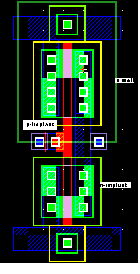
 

Basic MOS FET question

layout just represent mosfet.
we use self aligned process where gate is manufactured first and then doping is done for n+
Automatically only source and drain are created and region below gate is P-substrate only.

**broken link removed**

see above link for manufacturing details...


coming to layout point of view:
it looks like that it is complete n diffusion (even below poly) but it is not fabricated as such.
are below poly will be substrate only.

in real layout u will be having a complete n+ implant layer over mosfet.
active is first layer then you draw n+/p+ layer to create n+/P+ diffusion

Added after 4 minutes:

after poly is fabricated over p substrate then we do ion implantation of n+, so only source/drain get created and poly also get doped with n+.
doping poly with n+ is required for low resistivity purposes
 
Re: Basic MOS FET question

Thanks ankitgarg0312 for the good explanation.

I'd like to ask one more question, which is related. Outside the MOS FET, there is usually an implant region surrounding the FET (please see the attachment). For N MOSFET, a N Implant region and for P MOSFET, a P Imlant region is used. What is the reason for the implant?

Thanks.


ankitgarg0312 said:
layout just represent mosfet.
we use self aligned process where gate is manufactured first and then doping is done for n+
Automatically only source and drain are created and region below gate is P-substrate only.

**broken link removed**

see above link for manufacturing details...


coming to layout point of view:
it looks like that it is complete n diffusion (even below poly) but it is not fabricated as such.
are below poly will be substrate only.

in real layout u will be having a complete n+ implant layer over mosfet.
active is first layer then you draw n+/p+ layer to create n+/P+ diffusion

Added after 4 minutes:

after poly is fabricated over p substrate then we do ion implantation of n+, so only source/drain get created and poly also get doped with n+.
doping poly with n+ is required for low resistivity purposes
 

Basic MOS FET question

The implant represents the well. A PMOS is fabricated in a n-well. The n-type acts as substrate to the PMOS.
 

Re: Basic MOS FET question

The implant region for P MOS is actually P type, and for N MOS, the implant is N type. In P MOS layout, I can see that there is a N-well drawing as well as a P implant region. So I am pretty sure that implant is not meant for well.

Any other thoughts?

neils_arm_strong said:
The implant represents the well. A PMOS is fabricated in a n-well. The n-type acts as substrate to the PMOS.
 

Basic MOS FET question

implant is a layer used to specify N+ or P+

normally we use a active layer which is considered to be neutral then we cover it with n+/P+ implant layer to make it either N+/P+

in your diagram N-diff is acutually active layer which is surronded by N+ implant to make it N+ doped region.
N well are a seperate layer which is drawn around p+ implant to make a N-WELL in a pmos

Added after 5 minutes:

see attached diagram

28_1266807925.gif


Added after 2 minutes:

here upper part is Pmos and lower part is nmos.

pmos has a yellow P+ implant , which means pmos then a green colour nwell to show that it is made in nwell.
nmos has sperate nimplant surronding active area.

in both pmos and nmos active area is in middle with same colour (light green)

let me know for further info
 
Re: Basic MOS FET question

Very nice, ankitgarg0312. Your answer always gets to the point.

So really the implant layer is used to help to differentiate the P+ and N+ diffusion layer, as the diffusion layer is the same for both P+ and N+. Is it right to assume then that the shape of the implant layer is not critical, as long as it surrounds the active region, and the implant layer should not be transferred to any polygons on masks?

Thanks.


ankitgarg0312 said:
implant is a layer used to specify N+ or P+

normally we use a active layer which is considered to be neutral then we cover it with n+/P+ implant layer to make it either N+/P+

in your diagram N-diff is acutually active layer which is surronded by N+ implant to make it N+ doped region.
N well are a seperate layer which is drawn around p+ implant to make a N-WELL in a pmos

Added after 5 minutes:

see attached diagram

28_1266807925.gif


Added after 2 minutes:

here upper part is Pmos and lower part is nmos.

pmos has a yellow P+ implant , which means pmos then a green colour nwell to show that it is made in nwell.
nmos has sperate nimplant surronding active area.

in both pmos and nmos active area is in middle with same colour (light green)

let me know for further info
 

there are predefined rule by foundry known as DRC.
these rules determines minimum ensloure of diffusion by implant.

so if you are meeting their layout rules you can draw any shape , but practically you to make sure that you are not wasting area , not introducing any nonsense complexity in layout mask.
as this will effect your chip yields..

Added after 2 minutes:

making small notches/rectangles etc in layout affect your quality of layout as well as when it goes for final fabrication , you may get problems in yields..
so its always preferred to make clean and systematic layout .

it helps in integration of modules at top level also
 
CMOS foundry flows are designed to be self-aligned, the gate
poly is a "hard mask" for free, in a sense. To get the right
underlap of S, D under gate with a lightly doped S/D structure
an engineered spacer oxide and implant are used. You do not
get to draw mask-patterned S, D as a general rule. The last
process I worked on that allowed this was a 4um min gate
(self aligned), 10um if not self aligned.

If you draw the source / drain "stood off" from gate you can
get into things like failure to "hook up" the channel at low
VDS, making ugly distortion and RON-nonlinearity effects.
Some small amount of "can't-fail" underlap is a good thing,
though as little as acceptable helps Cgdo/Cgso and breakdown.
 

Status
Not open for further replies.

Similar threads

Part and Inventory Search

Welcome to EDABoard.com

Sponsor

Back
Top