Continue to Site

Welcome to EDAboard.com

Welcome to our site! EDAboard.com is an international Electronics Discussion Forum focused on EDA software, circuits, schematics, books, theory, papers, asic, pld, 8051, DSP, Network, RF, Analog Design, PCB, Service Manuals... and a whole lot more! To participate you need to register. Registration is free. Click here to register now.

Help designing Buck Converter in PSpice

Status
Not open for further replies.

jurassicbond

Newbie level 1
Joined
Nov 30, 2009
Messages
1
Helped
0
Reputation
0
Reaction score
0
Trophy points
1,281
Activity points
1,296
I'm trying to design a buck converter in PSpice for class and I followed the design found here on page 3.
https://www.scribd.com/doc/6834949/dc-to-dc-converters-using-ORCAD-spice
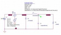
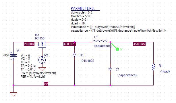
My circuit is here:


and the plot of the capacitor voltage is here:


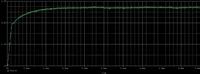
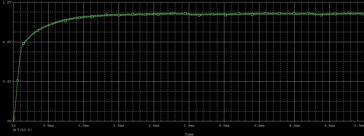
The capacitor voltage is around 1.2 volts when it should be around 10 Volts. For some reason, the Capacitor voltage only changes if I change the parameters of the control voltage, but if I change the input voltage nothing changes. I can't figure out what I'm doing wrong. I'm pretty sure that I followed the book correctly and my design is right, but I'm probably doing something wrong in PSpice since it's been a long time since I last used it.
 

You need to connect negative pin of V2 source to MOSFET source pin instead of GND.
Hope this helps.
 
or increase the magnitude of V2 to 15V
This doesn't result in correct switching operation. V2 has to be at least 5 to 10 V above input voltage V1, which would exceed FET maximum Vgs ratings (although the simulation models possibly ignores the dangerous operation condition).

As a general question, do you intend to simulate a real-world buck converter or a simplified functional model? For the real converter, a feasible gate drive method should be included with the simulation, because the actual gate voltage waveform affects the buck converter's efficiency and switching behaviour considerably.
 

And u must also pay more attention to the working mode of MOSFET,what we want is switch, not a resistor,right?
 

pspice is not a good choice for simulating a switching circuit.
it will take too long a time for simulation.
hock
 
You need to study how to turn on P-mos to the N-mos. The left of the inductor, L1, is 20V when the switch is supposedly first turned on. For N-mos, the gate voltage needs to be higher than source voltage.

In this case, the gate voltage turns on the N-mos, but as soon as N-mos conducts, it is quickly turned off. After you study the N-mos to P-mos or how to bias them, you can go to Maxim website. There is a pretty good tutorial.
 

u done one mistake tat is connecting the negative end of gate pulse to ground. u have to connect Vgs instead of gnd . connect -ve of gate pulse to mosfet tat connecting to diode
 

Status
Not open for further replies.

Similar threads

Part and Inventory Search

Welcome to EDABoard.com

Sponsor

Back
Top