umery2k75
Advanced Member level 1
lm2937 replacement
I actually had a development board, in which one SMT IC was damaged. I wanted to replace the IC, but unfortunately doing so, I had permenantly damaged the LQFP 64 IC legs and now the board is gone and my all work is stuck now. I email to Europe to their company to send me another one, but those guys are not replying. Even though the board cost around 35US$ with 75US$ of shipping. Beside all this, I want to have the board as soon as possible, so I will be placing a order soon, as I have talk with that company.
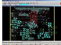
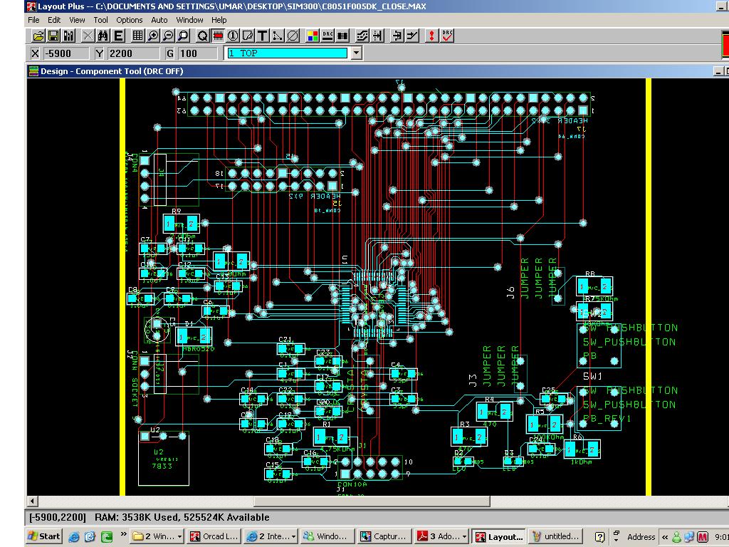
But what I have seen is that their PCB was designed very good. Very nice routing and few VIAS, my layout board is very bad comparative to the board I have on my hand. Every thing very nice done. Few VIAS, where as in mine, there are hell lot of vias. The tracks also runs at 45' in the board, but in Orcad, the lines are mostly either horizontal or vertical. Every where I see copper pours polygon. I don't know how to make such a nice PCB in Orcad. First tell me how can I restrict the VIAS. In my screwed up development board, there's only 4 VIAS inside the 64 pin controller, but in my orcad design there are 15 VIAS inside the microcontroller.
Added after 2 minutes:
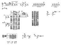
This is the schematic of the board, if you see, it's really simple.
I actually had a development board, in which one SMT IC was damaged. I wanted to replace the IC, but unfortunately doing so, I had permenantly damaged the LQFP 64 IC legs and now the board is gone and my all work is stuck now. I email to Europe to their company to send me another one, but those guys are not replying. Even though the board cost around 35US$ with 75US$ of shipping. Beside all this, I want to have the board as soon as possible, so I will be placing a order soon, as I have talk with that company.
But what I have seen is that their PCB was designed very good. Very nice routing and few VIAS, my layout board is very bad comparative to the board I have on my hand. Every thing very nice done. Few VIAS, where as in mine, there are hell lot of vias. The tracks also runs at 45' in the board, but in Orcad, the lines are mostly either horizontal or vertical. Every where I see copper pours polygon. I don't know how to make such a nice PCB in Orcad. First tell me how can I restrict the VIAS. In my screwed up development board, there's only 4 VIAS inside the 64 pin controller, but in my orcad design there are 15 VIAS inside the microcontroller.
Added after 2 minutes:
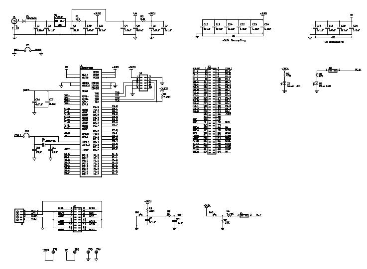
This is the schematic of the board, if you see, it's really simple.