Continue to Site

Welcome to EDAboard.com

Welcome to our site! EDAboard.com is an international Electronics Discussion Forum focused on EDA software, circuits, schematics, books, theory, papers, asic, pld, 8051, DSP, Network, RF, Analog Design, PCB, Service Manuals... and a whole lot more! To participate you need to register. Registration is free. Click here to register now.

Bandgap not settleing to zero..when...

Status
Not open for further replies.

bharatsmile2007

Full Member level 3
Joined
Sep 19, 2007
Messages
179
Helped
1
Reputation
2
Reaction score
1
Trophy points
1,298
Activity points
2,306
Hi all,

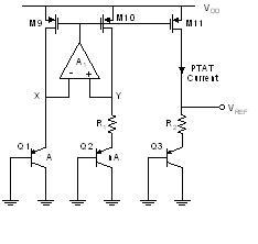
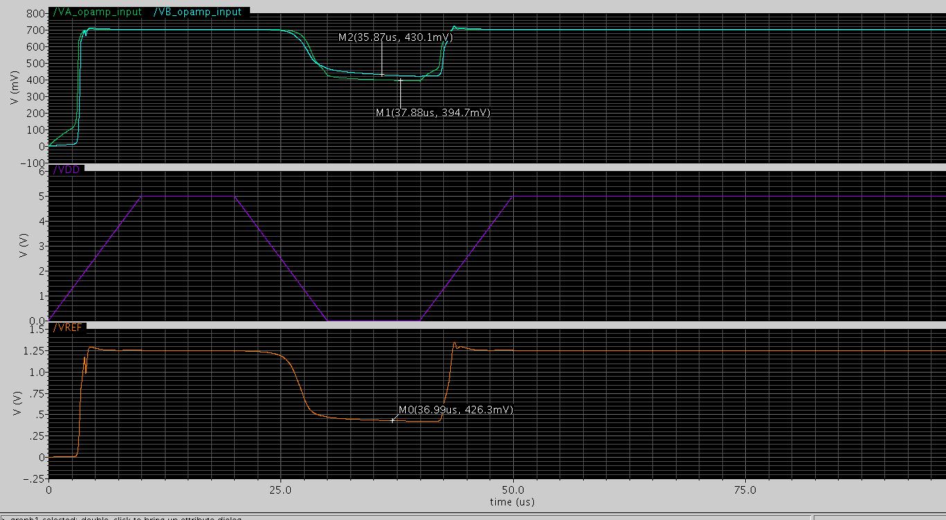
In a BGR.when given a pwl to vdd,varying from 5V to 0V.

when vdd is 5V Vref (output) is 1.26V,
when vdd is zero Vref is around 0.5V.

Can any one let me know what would be the possible reason for Vref not settling to zero volts?

pwl was given a rise/fall delay 10u and pulse width 10u...

Thanks

51_1231415763.jpg


3_1231473171.jpg
 

I'd guess this is because you have no output load at the Vref output. With vdd=0, Vref falls until the npn diode (at about 400mV) gets so high resistivity (its pull-down current so low), that it would take a rather long time to fall to zero (high relaxation time). You'd probably see this if either you make the vdd=0 phase very long (order of seconds) or you provide an output load.

HTH, erikl
 
Once VREF falls below a diode drop, Q3 shuts off and is high impedance. Basically, the VREF node will be clamped at a diode drop with respect to Q3/ With the VREF node being high impedance you have no way to discharge that node, excpet for leakage current. It will eventually discharge if you give it a long time. If you put a small load on VREF, it will discharge to zero. If you need it to discharge to zero immediately when VIN collapes, you'll have to put some sort of pull down on that node. There is nothing wrong with the circuit as it is.
 

Hi all,

I tried connecting the load and given more time to settle the ciruit around 1sec...still i see the same....

Load around 500pF...

any other problem would to be the cause for this...

Thanks
 

bharatsmile2007 said:
Hi all,

I tried connecting the load and given more time to settle the ciruit around 1sec...still i see the same....

Load around 500pF...

any other problem would to be the cause for this...

Thanks

Hi bharatsmile,
with such a high capacitive load it gets even worse, because it will take more time to discharge this additional capacitor. Remove the cap and instead add a resistive load in the order of 1MOhm.
Thanks! erikl.
 

Thanks erikl..

when i connected resistive load its getting settled to zero...But in real scenario the load will be capacitive right?
 

bharatsmile2007 said:
But in real scenario the load will be capacitive right?
If you want the output to decharge down to GND , also in real life you have to add either a (high) resistor, or you pull this output down to GND with an extra nfet transistor controlled by your disable signal. A minimum size nfet is sufficient.
 

An additional transistor which performs enable/disable helps!
 

Status
Not open for further replies.

Part and Inventory Search

Welcome to EDABoard.com

Sponsor

Back
Top