Continue to Site

Welcome to EDAboard.com

Welcome to our site! EDAboard.com is an international Electronics Discussion Forum focused on EDA software, circuits, schematics, books, theory, papers, asic, pld, 8051, DSP, Network, RF, Analog Design, PCB, Service Manuals... and a whole lot more! To participate you need to register. Registration is free. Click here to register now.

[SOLVED] How do you deal with GND PAD to VSS Rail?

Status
Not open for further replies.

prcken

Advanced Member level 1
Joined
Nov 1, 2006
Messages
419
Helped
41
Reputation
82
Reaction score
37
Trophy points
1,308
Location
Shanghai
Activity points
4,059
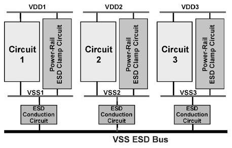
will you connect GND PAD through a dual diode to VSS rail or just connect to VSS rail directlly?
what's the pros and cons of both methods?
thanks!!!

0_1230448641.jpg
:?:
 

0_1230448641.jpg

prcken said:
... connect GND PAD through a dual diode to VSS rail or just connect to VSS rail directlly?
what's the pros and cons of both methods?
IMHO this depends on the "potential status" of your GNDLNA resp. GuardringLNA pins:
If you have separate GND regions on chip which are isolated from each other - either by SOI, STI or by separate n-wells - you should use the diode protection scheme. If your different GND pin connections, however, are connected anyway by the same (p)-substrate, then the protection diodes aren't necessary, as there exists a (enough) low-resistive connection via the substrate.
 

erikl said:
IMHO this depends on the "potential status" of your GNDLNA resp. GuardringLNA pins:
If you have separate GND regions on chip which are isolated from each other - either by SOI, STI or by separate n-wells - you should use the diode protection scheme. If your different GND pin connections, however, are connected anyway by the same (p)-substrate, then the protection diodes aren't necessary, as there exists a (enough) low-resistive connection via the substrate.


hey, erikl, thanks for your answer
what does 'IMHO' mean?
you are absolutely right, the dual diode to the Vss rail is used in multiple power sets in Soc, the Vss rail is so called ESD bus. just like the picture shows, but the vss1 vss2 just a single pad, not a rail
61_1230552279.jpg
 

prcken said:
hey, erikl, thanks for your answer
what does 'IMHO' mean?
Hi prcken, thanks for your answer, too, and for the picture!
About 'IMHO' you'll easily find out via Google or Wikipedia (In My Humble Opinion) ;-)
 

    prcken

    Points: 2
    Helpful Answer Positive Rating
I think Erikl pretty much answered it for you, but I would like to add a minor comment.

The anti-parallel diodes between two VSS's generally serve the purpose of isolating the domains for noise.
As Erikl mentions, if you have two VSS's that are relatively isolated because of SOI, or some other technology...than it may be beneficial to keep them separate by use of the diodes.

However, if they are in the same p-substrate, consider a few factors: your subtrate resistivity and the overall size of P+ tap of the two VSS's.
If its high resistivity or if your RF VSS (or whatever the non-ESD-VSS bus is) is a small domain in terms of total area and so forth, you may just want to use the diodes as you may still be getting some isolation. This is very subjective however, and I have generally found that the isolation is not that great and the ESD performance can be improved dramatically by simply shorting the VSS's together at the pad.
I say at the pad because you can get some benefit of kelvin type connections and controlling your noise current paths.

Its all part of your chip level signal integrity.
 

srftech said:
.............
However, if they are in the same p-substrate, consider a few factors: your subtrate resistivity and the overall size of P+ tap of the two VSS's.
If its high resistivity or if your RF VSS (or whatever the non-ESD-VSS bus is) is a small domain in terms of total area and so forth, you may just want to use the .......
Its all part of your chip level signal integrity.

hey, thanks for your nice proffesional comments
what I have done is connect the cathode of all the power clamps and ggnmos, also diode at the RF pads directly to the VSS ESD bus, and all GND pads via dual diode connect to VSS ESD bus, too. VSS ESD bus floating, and VSS ESD bus in different blocks are connected by dual diode.
Do you think is that OK?
 

Well, I am uncertain what you mean by cathode of the power clamps and ggnmos, but I assume you mean the source nodes of the ggnmos's or power clamps (assuming active nmos). Correct me if I am wrong.

I think what you have done is "ok", but I do not believe in ever letting the ESD bus float (though certain designs have merited it in the past...others do not have an explicit ESD bus)...My preference and recommendation is that you pick one of your larger grounds that is tied to substrate, and use that as your global ESD bus.

Again, most designs do not usually have the luxury of a dedicated ESD bus, so its good not to get in the habit of using one.
 

    prcken

    Points: 2
    Helpful Answer Positive Rating
srftech said:
Well, I am uncertain what you mean by cathode of the power clamps and ggnmos, but I assume you mean the source nodes of the ggnmos's or power clamps (assuming active nmos). ........

yes, that's what i meant
the initial purpose to let the VSS ESD bus floating is to aviod the GND pads being affected by a fixed voltage potential at VSS ESD bus to Substrate. for better noise isolation from the substrate.
 

Hi prcken,
I understand what you mean about isolating noise from the substrate but here is something else to consider.

If I understand correctly, your substrate is apparently floating because you floated the only major bus connected to it (VSS_ESD), this because you do not want any GND pads tied to the substrate. OK, but now since substrate is floating noise will propagate through it more readily between your different domains with more energy than if you had a low impedance path to pick up some of the carriers/noise energy.

If you have space, I would add extra GND pads strictly for the Vss_ESD bus and substrate taps that can be down bonded to a GND flag in your package. This would actually help improve dramatically the noise in your substrate between domains.

Just a thought. :)
 

srftech said:
Hi prcken,
...... but now since substrate is floating noise will propagate through it more readily between your different domains with more energy than if you had a low impedance path to pick up some of the carriers/noise energy.

If you have space, I would add extra GND pads strictly for the Vss_ESD bus and substrate taps that can be down bonded to a GND flag in your package. ..............
Just a thought. :)

hey, thanks
really appreciate..
i will add extra GND pads in each domain for the sub so that can be down bonded to physical ground.
 

Just a suggestion.
Since multiple power domain is used, VDD1, VDD2 and VDD3, maybe the ESD protection between those different VDDs should be considered, except the Vss issue.
 

wangyufn said:
Just a suggestion.
....... maybe the ESD protection between those different VDDs should be considered, ........

Yes, you are quite right, the VDD pads are seperated from each other
 

Status
Not open for further replies.

Part and Inventory Search

Welcome to EDABoard.com

Sponsor

Back
Top