quattro44
Newbie level 4
allegro spb
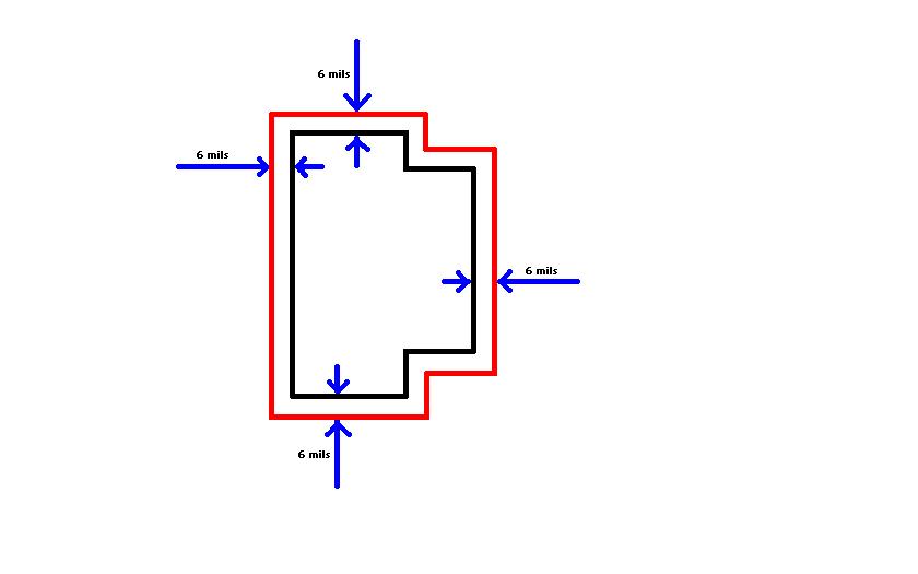
Hi to all, I am a new user of Cadence Allegro SPB 16.0 but I have been doing PCB layouts for quite a while already using another software(Zuken CR-5000). I would like to know how i can go about making irregularly shaped pad stacks in Allegro. And if there is anyone that can give me tutorial videos or documents for Cadence Allegro, I would greatly appreciate it. Our company is tight on budget so they decided not to get a professional Cadence Allegro trainor for us. Thank you very much.
Hi to all, I am a new user of Cadence Allegro SPB 16.0 but I have been doing PCB layouts for quite a while already using another software(Zuken CR-5000). I would like to know how i can go about making irregularly shaped pad stacks in Allegro. And if there is anyone that can give me tutorial videos or documents for Cadence Allegro, I would greatly appreciate it. Our company is tight on budget so they decided not to get a professional Cadence Allegro trainor for us. Thank you very much.