sykab
Member level 2
Hi,
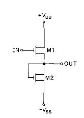
I'm using a souce follower, as you can see in the image, to do the output stage of an OPAMP.
I put a NMOS and a PMOS, that are, in the image, M2 and M1, respectively.
Am I right? I hope so, because it works and the opamp works well.
I'm using a souce follower, as you can see in the image, to do the output stage of an OPAMP.
I put a NMOS and a PMOS, that are, in the image, M2 and M1, respectively.
Am I right? I hope so, because it works and the opamp works well.
