wang.yuanzhuo
Junior Member level 2
glitch in current steering dac
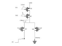
the circuit cell
Added after 12 minutes:
Added after 11 minutes:
I'm design a DAC used the classic current steering circuit. But I need a large fixed output voltage range.
It cause large step in the common source node of switch M3 and M4 (>300mv), also a large glitch at the bias node vb1. The loading of vb1 is heavy,so it can't recovery quickly and my setting is bad. I've add large cap at the node of vb1 and vb2, but still can't supress the glitch well.
Could any one give me some suggestion to supress the glitch or make the recovery of vb1 quickly?
Thank a lot
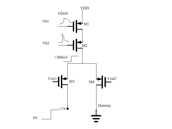