Continue to Site

Welcome to EDAboard.com

Welcome to our site! EDAboard.com is an international Electronics Discussion Forum focused on EDA software, circuits, schematics, books, theory, papers, asic, pld, 8051, DSP, Network, RF, Analog Design, PCB, Service Manuals... and a whole lot more! To participate you need to register. Registration is free. Click here to register now.

Power line layout for AVDD line

Status
Not open for further replies.

electronXwork

Member level 3
Joined
Apr 27, 2007
Messages
56
Helped
4
Reputation
8
Reaction score
2
Trophy points
1,288
Activity points
1,623
Power line layout

Hi all,

Please see the attached file for reference.
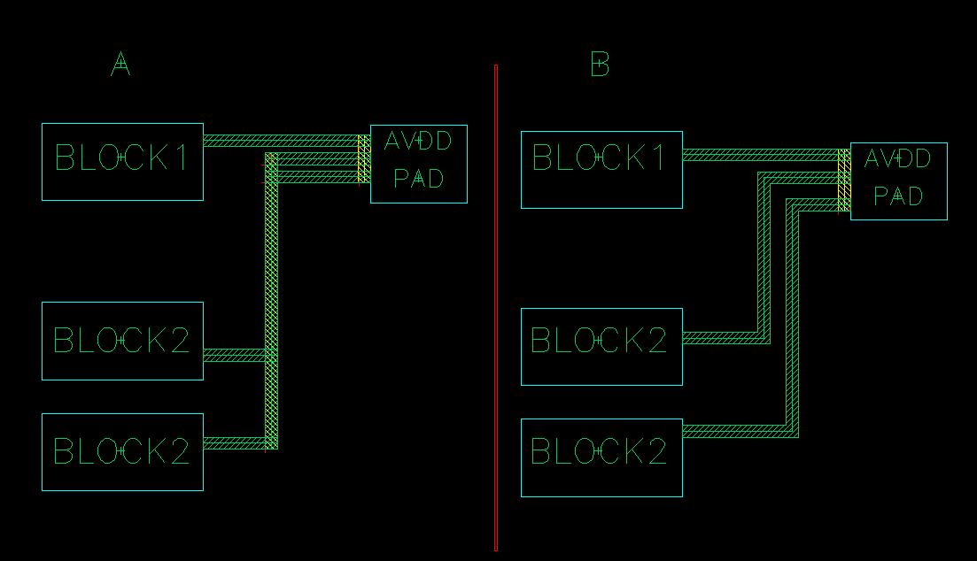
Initially I layout A for AVDD line but I was requested to do layout B. In A, notice the vertical line, to save space I overlaped M1 and M2 w/ via12 on them. In B, I was instructed to have a dedicated AVDD line for each block to the pad but by doing this I would not have enough space anymore for the other lines.

Please tell me why do they insisted B? I think A has the same current distribution as B. Does noise is related? Because I am thinking that it is possible that the line in block2 may accumulate noise and might be passed on to block3 or vice versa. Please clarify and if you have other reasons I will be thankful if you share them.

This is also applied to AVSS lines.


Re: Power line layout

It will to minimise the noise being feed into each block. Block A for example may be a noisy digital cell whilst block C may need a quiter signal. By staring them back to the pad without overlaping minimizes the effects of noise polution. You could do block B in met2 use a met3 sheild and then a met4.
 
Re: Power line layout

k_90 said:
You could do block B in met2 use a met3 sheild and then a met4.

This layout is three metal process only...
 

Re: Power line layout

use 1M and 3M in routing the power lines.
if noise is really an issue, put 2M in between them and connect it to the ground.
The 3 parallel plates will act as a parasitic capacitor ( 1M to ground and 3M to ground).
These parasitic caps is very useful in power lines as they bypass noise.

Added after 4 minutes:

if the two lower blocks are the same, i think there is no need for them to separate the power lines. You should only do that (power separation), if and only if, another block (should i say noisy block) is connected to either of them.
 

Re: Power line layout

Im sorry for the mistake on the drawing. the blocks are block1, block2, and block3 from top to bottom
 

Re: Power line layout

Yes,it is better to maintain seperate power line for each block from the power pad.
It is not a issue of noise,it is a issue of current rating.If you cobined the two power lines,you don't know which one is drawing more current.If enogh current is not reached the block,it may mal functioned.
 

Power line layout

I think K_90 is right!
power line should be one point connected.
 

Re: Power line layout

if for example in a ADC ckt I encountered AVDD3L, AVDD3R, AVSS3L, AVSS3R these lines are in the same ADC block. AVDD3L and AVDD3R are going to the same I/O pad same as for AVSS3L and AVSS3R. Do i still have to route them seperately going to the pad?
 

Re: Power line layout

The seperate power lines as provided in 'B' is recommended.
It depends o the IR drop also.
1.The Block 2 which has less routing length will have less IR Drop.
2.If the total current drawn by block 2 is greater than block 3 there also the approach B is correct.
This type of routing is called 'star connection'.i.e though two blocks share the same AVDD they will be shorted only at the PAD.

Please express views if i m wrong.
 

Re: Power line layout

Yes what ever SP24 said is right.

The first conept that recomending the B is Noise and second conept is IR drop.
Whenever you are doing a power routing you need remind these two concepts.

If you really feel, you want to have space it's better you decrease width of the each metal line and use stacked metal to satisfy the current rating. By that way you can save you space. This is possible if you don't have any other routing on that. Please give me feedback if i am wrong. Thank You.
 

Re: Power line layout

Separate the Analog ,semi and Digital power lines and connect all these at nearer to the PAD.
 

Power line layout

Very Useful Documentation ...
Thankx a lot.

Very Nice.
 

Status
Not open for further replies.

Part and Inventory Search

Welcome to EDABoard.com

Sponsor

Back
Top