jimmyshu
Newbie level 6
explain current sources
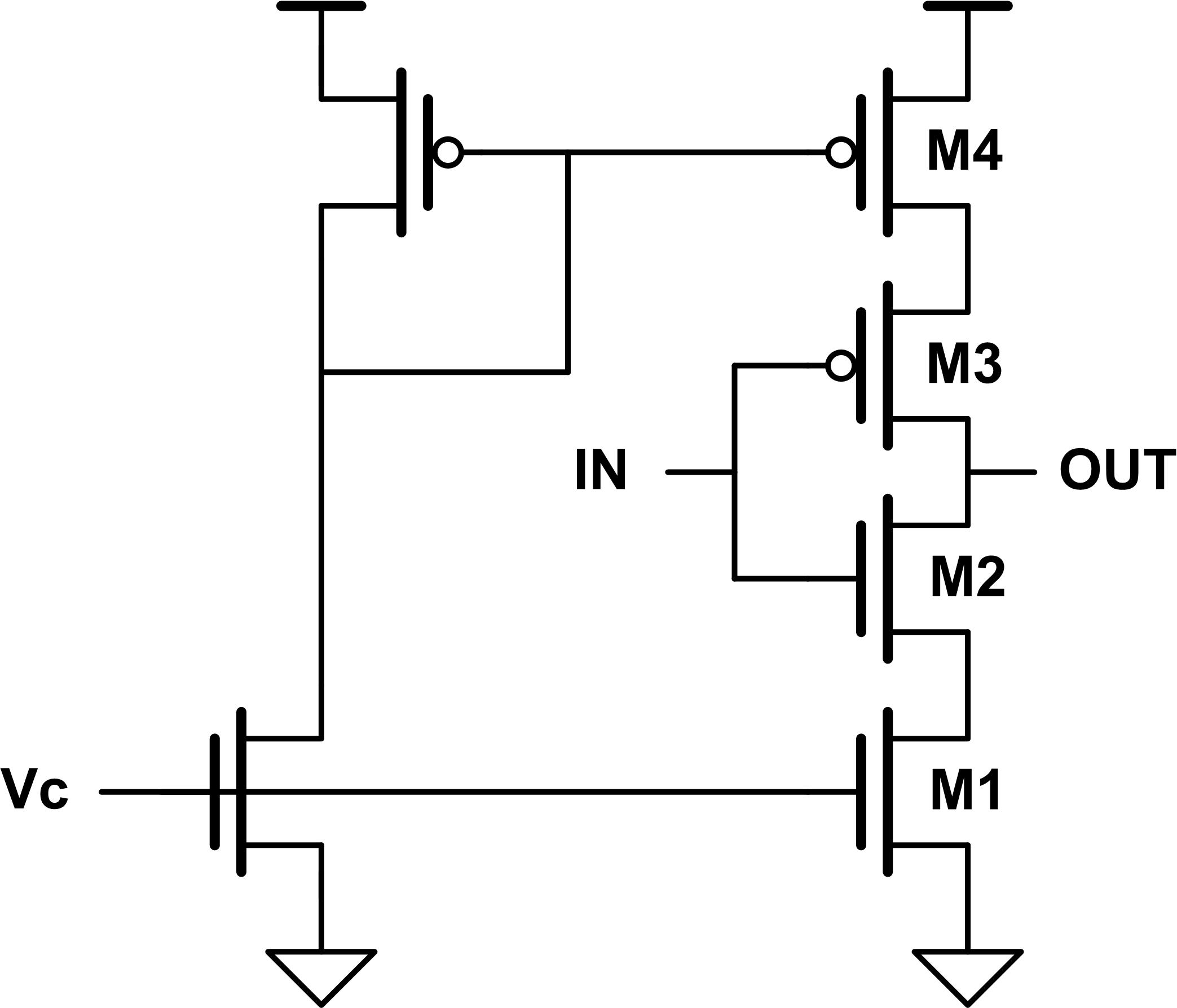
The circuit is shown in Fig 1. as you can see, this is a inverter, but I don't know why M3 is used in here. Obviously, M3 is a current source. Is it for biasing the inverter?
The circuit is a basic unit of a chip. In that chip a lot of digital circuits, such as AND, OR, D-Latch and so on, is similar to this inverter biased by current sources. By the way, the chip is extreme low-power, the total supply current is only 4uA including analog parts and digital parts. So I guess maybe it is for limiting the peak current. As I know, when vin is in switch-point, pmos and nmos are all on to produce a large current. So in this circuit the maxmum current is limited by source current, and we can design a very small biasing current source such as 0.1uA.
This is my guess, and I don't know whether it is right.
Welcome to criticize!
Thank you so much!