Continue to Site

Welcome to EDAboard.com

Welcome to our site! EDAboard.com is an international Electronics Discussion Forum focused on EDA software, circuits, schematics, books, theory, papers, asic, pld, 8051, DSP, Network, RF, Analog Design, PCB, Service Manuals... and a whole lot more! To participate you need to register. Registration is free. Click here to register now.

How to set the output voltage correctly in OTA design?

Status
Not open for further replies.

diemilio

Full Member level 6
Joined
Sep 19, 2006
Messages
383
Helped
64
Reputation
126
Reaction score
15
Trophy points
1,298
Location
Framingham, MA
Activity points
3,797
Hello everyone!!

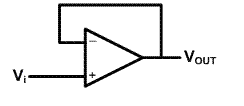
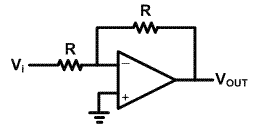
When designing an OTA, one of the most difficult taks is to set the output voltage to a desired value (when driving capacitive loads). I've heard that there are feedback approaches to set this output voltage. Could someone please explain me how can I do this???


Thanks,

diemilio
 

output offset values

Hi

What is your OTA structure????
If you have a single ended one, and you want to use the OTA in a negative feedback configuration, then this configuration itself can set the output voltage (should be design for suitable qualification). But if you have a fully differential configuration, you need a CMFB (common-mode feedback) circuit that its structure is depending on your OTA architecture..
 

re output offset

Is a single ended OTA.

What I don't understand is how feedback would set the output offset value to Vdd/2
 

Re: output offset

There are many architectures for applying negative feedback to an OTA. I explain you two of simplest (working for special applications). The first one is the simple negative feedback with the architecture below:

34_1192779345.gif


In this case as you know the output voltage follows the input one (acting as a voltage buffer) according to the relationship below:

Vout = Av(Vp – Vn) => (Vp – Vn) = Vout/Av

For Av with large enough value Vout/Av app. equal to zero and so Vp app. equal to Vn = Vout.

So in this case the output voltage have the common-mode value equal to the common-mode of input signal and so the OTA should design for equal input and output common mode voltages.

The next common architecture is as follows:

88_1192779375.gif


In this case with equal resistances, the circuit is also acting as buffer and the input and output common-mode voltages are equal. If you need different input and output common-mode voltages, you must choose suitable values for resistances, and you may need an additional circuitry for setting the OTA input common-mode voltage.
 

    diemilio

    Points: 2
    Helpful Answer Positive Rating
Status
Not open for further replies.

Part and Inventory Search

Welcome to EDABoard.com

Sponsor

Back
Top