Continue to Site

Welcome to EDAboard.com

Welcome to our site! EDAboard.com is an international Electronics Discussion Forum focused on EDA software, circuits, schematics, books, theory, papers, asic, pld, 8051, DSP, Network, RF, Analog Design, PCB, Service Manuals... and a whole lot more! To participate you need to register. Registration is free. Click here to register now.

Why we insert a look-up latch in a chain when the chain is crossing clock domain?

Status
Not open for further replies.

lty

Junior Member level 3
Joined
May 24, 2004
Messages
28
Helped
7
Reputation
14
Reaction score
4
Trophy points
1,283
Activity points
214
I am studying the ATPG recently.
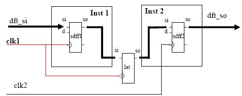
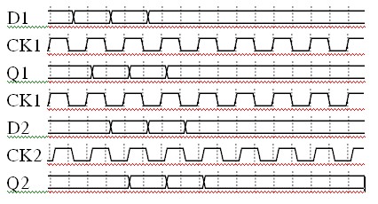
I try to understand why insert a look-up latch in a chain when the chain is crossing clock domain.
Can anybody give some answer about this, or give some reference?
 

lock up latch diagram

A lock up latch is used to deal with t skew....when chains in differernt clock donmains cross,it is necessary to use a lock up latch to avoid problems due to skew..also it is used when we hav flip flops operating on t +ve edge and some operating on the -ve edge,then lock up latches r used in between them

Added after 1 minutes:

I don have any material right now...wil try to provide u with it as soon as i get some!
 
lock-up latch diagram

34_1167020400.JPG

Hi, thank you for your answer.
I know something from your answer, could you check my idea is right?

the scan chain cross the register dff1 and dff2, the dff1, dff2 is clocked by clk1, and clk2. clk1, clk2 belong to different clock domains.
because they are different clock domain, so they are belong to different clock tree, their clock path are not balanced.
When do ATPG, the test clock controls the dff1 and dff2, the test clk go to dff1 through clk1 clock tree, go to dff2 through clk2 clock tree. so there may be a big clock skew between dff1 and dff2.
when we insert a lockup latch between them, we can improve the hold timing between dff1 and dff2, avoid timing violation.

thank you!

Added after 55 minutes:

add a timing diagram.

Q1 is the output of dff1,
D2 is the output of lock-up latch,
when not insert lockup latch, the dff2 need catch the data Q1, because of skew between clk1 and clk2, there may be hold violation.
when insert lockup latch, the dff2 catch the data D2, it is more easy to cach data D2 for DFF2, because the lockup latch delays the Q1 for a half clock period.

71_1167024445.jpg
 
Status
Not open for further replies.

Part and Inventory Search

Welcome to EDABoard.com

Sponsor

Back
Top