Continue to Site

Welcome to EDAboard.com

Welcome to our site! EDAboard.com is an international Electronics Discussion Forum focused on EDA software, circuits, schematics, books, theory, papers, asic, pld, 8051, DSP, Network, RF, Analog Design, PCB, Service Manuals... and a whole lot more! To participate you need to register. Registration is free. Click here to register now.

need your advice about this layout.

Status
Not open for further replies.
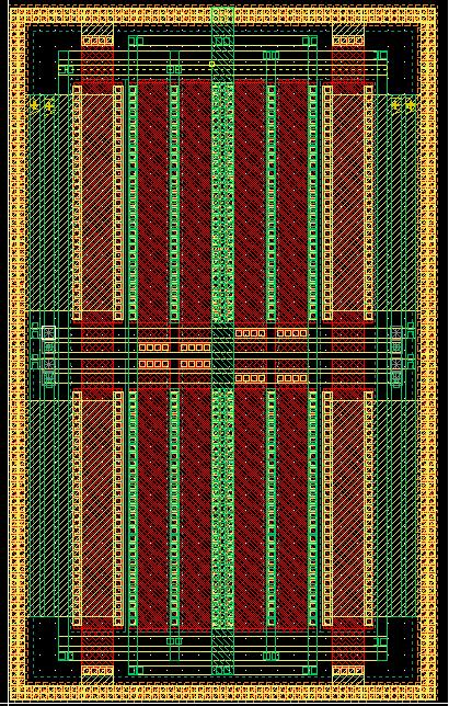
This is my improved layout. Any advices are appreciated.
Thanks a lot for the reply all of above.

**broken link removed**
 

good look,but in my opinion,you'd better use the min rule,your layout watse some space,and what we need is reduce the cost :)
 

Hi sophiefans,

This is a much better artwork compare to previous version. :D
However, a few comments from me, FYI:
1. You may not need to do guard ring on the whole opamp. Guard ring those sensitive transistor, such as NMOS diff pair is sufficient. Let the guard ring of whole block (if needed) done by people in charge of top-level integration.
2. Not only NMOS, guard ring should be placed to PMOS too. For this particular layout, you may not need to do so, as the PMOS size is very small. For big PMOS, guard ring ensure proper bulk bias and reduces mismatch.
3. If this layout will be reused quite frequently, I still strongly suggest that output pin place on the right. This is because, from top level view, analog signals will always propagate from left to right, or top to bottom or vice versa. It is seldom to have 90 degree bend, unless area limitation.
 

in the differential pair routings also should be symmetric
ur routings can be done in a better way still
 

try to make ur diff pair balance and add more contacts to the inputs...
i hope this image helps...
observe the balanced wiring ang device placement...
avoid also passing other connections thru the opamp...
this may occupy more space but needed when sensitive matching is required...


82_1161145261.JPG
[/img]
 

    sophiefans

    Points: 2
    Helpful Answer Positive Rating
ya thats correct
the input to gate contacts should be increased.
and also obsorve the routing symmetry even
 

Yes, it looks so symmetry & beautiful.
But, could somebody explain that where i should use wide metel wire or where i sould use narrow wire except for current density consideration?

such as :wide metel=small sheet resister&big parasitic capacitance
Is this right? Or some other consideration?

thanks
regards
sphiefans
 

You need to use wide metal for:
1. High current density path
2. Low impedance path (especially important for power line and ESD ring/paths).

wide metal gives smaller metal resistance. You have additional parasitic capacitance on wide metal only if something are under the wide metal. If there is nothing under it (which is the case for power lines that I suggest), wider metal does not add any additional parasitic caps.
 

narrow lines/wires are acceptable for gate connections... :D
 

I am also layouting my first circuit.Can the metal cross the ploy?
 

Cant the criss-crossing of in1 and in2 (45°) be changed??!!!
I understand that there is no current flowing into the gates.. but still as a designer i would be very wary of fringe capacitances that such angles induce... :cry:

Also is it not a good idea to draw both the diff inputs with the same metal?? The noise implications will be different...

The paths can be matched through different methods..
 

now the improved layout looks pretty good, one more commnents for that, please add at least 2 vias/ contacts if there is enough room.
 

still no answer as to why the input lines are crossing at 45°....
 

yes , matel can cross poly .

they are vertically seperated layers
 

hi

metal crossing the poly is not allowed as per my understanding

regards

analyout
 

CISSE what kind of a question is that? Do you have the technology manual or you are just making an exercise?

Normaly, Polysilicone is right on top of the substrate whereas first metal layer is 0.5 to 2 microns higher! That means that in the real world M1 is on the first floor and Poly in on the ground Floor!

I would suggest to check the page with all the metals you are using and that has accurate description of the distance between them . Try to remember that layout is just overlaping masks for injecting different matterials but NOT at the same time and NOT at the same level.

If you have more to ask please do, I would be glad to help - and everyone else in here I presume!
D.
 

oh,i mean the cross in space,not at the same plane face.:D
 

analayout said:
hi

metal crossing the poly is not allowed as per my understanding

regards

analyout

WHY ???
 

offtopic:

How did you create this image/layout?
 

sophiefans said:
It is an normal OP AMP with differential input. The schematic lies in the right lower quadrant.

This is my fist layout which has passed DRC. I don't know what do you think about it. Could you tell me the mistakes you have found?

Thanks in advance.
sophiefans.

**broken link removed**

Hi there,

In my point of view if you really need a good matching between your paired transistors you need to add dummies on both sides. also make sure that the substrate contact is not only connected on one side of the transistor, you should surround it with psub ring.

The input lines if its noisy line..makes sure you put them in shielded lines that is connected to gnd and put as much polycontacts as necessarry.

capacitor you can changed the aspect ratio(you can stretch and make it rectangular not square).

Make your Supply and ground line wide...ask your designer how much current do you need to those...and you can compute the VDD/GND width look at the current handling capabilities of each metal in your design rule.

Also take out those two lines passing the transistor wire them out of the active area

I hope this help you.

cheers
 

Status
Not open for further replies.

Part and Inventory Search

Welcome to EDABoard.com

Sponsor

Back
Top