Continue to Site

Welcome to EDAboard.com

Welcome to our site! EDAboard.com is an international Electronics Discussion Forum focused on EDA software, circuits, schematics, books, theory, papers, asic, pld, 8051, DSP, Network, RF, Analog Design, PCB, Service Manuals... and a whole lot more! To participate you need to register. Registration is free. Click here to register now.

FRG-4 BFO combined with PLL fails

Status
Not open for further replies.

neazoi

Advanced Member level 6
Joined
Jan 5, 2008
Messages
4,119
Helped
13
Reputation
26
Reaction score
15
Trophy points
1,318
Location
Greece
Activity points
36,918
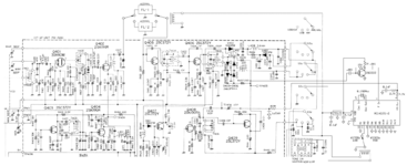
I am trying to lock the BFO of the FRG-7 (Yaesu) and the design is shown attached.
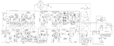
Whereas it locks fine, The audio tones are distorted (ringing). This happens on higher level signals not on lower.
This is shown in this video
The same ringing happens when I switch from USB to LSB and vice versa, for 1 second.
I noticed when I changed the loop capacitor on pin 4 of the PLL to higher value, the ringing becomes of lower frequency.

I do not know what is going on, any help?
 

Attachments

  • my_frg-9_mods3.PNG
    my_frg-9_mods3.PNG
    514.5 KB · Views: 142

Most likely T406 is off tune or one of the capacitors around it has shifted value slightly. From your description, the PLL is struggling to lock and is hunting until it manages.

I do not have the calibration procedure for that receiver but generally it you measure the PLL control voltage at the right side of the 820K resistor is should shift a little amount each side of half supply voltage as you switch one sideband to the other.

Brian.
 

    neazoi

    Points: 2
    Helpful Answer Positive Rating
Most likely T406 is off tune or one of the capacitors around it has shifted value slightly. From your description, the PLL is struggling to lock and is hunting until it manages.

I do not have the calibration procedure for that receiver but generally it you measure the PLL control voltage at the right side of the 820K resistor is should shift a little amount each side of half supply voltage as you switch one sideband to the other.

Brian.
Hi Brian,
I measure the voltage at that 820k and it is 3.67v at usb (bfo freq 453khz) and 4.31v at lsb (bfo freq 457khz). VCC to the pll is 5v.
The way I tuned T406 is at 460khz, then I let the pll bring this back to the 453 and 457khz.
Does it seem right to you or shall I tube the transformer a different way?
 

Seems that the BFO frequency is modulated my the demodulated IF signal when the RF signal is stronger. When you switch the attenuator from DX to Local, sounds better.
The reason could be that the product detector diodes (D403, D404, D405, D406) are not identical (maybe one of them lose the initial characteristics).
I would recommend to replace all these old Germanium diodes in the product detector (1N60) with new Schottky diodes. For example with: 2x BAT54S, 2x BAT64-05, or any other pair of RF Schottky diodes. Have to be careful how they are connected inside of the package.
 

    neazoi

    Points: 2
    Helpful Answer Positive Rating
Seems that the BFO frequency is modulated my the demodulated IF signal when the RF signal is stronger. When you switch the attenuator from DX to Local, sounds better.
The reason could be that the product detector diodes (D403, D404, D405, D406) are not identical (maybe one of them lose the initial characteristics).
I would recommend to replace all these old Germanium diodes in the product detector (1N60) with new Schottky diodes. For example with: 2x BAT54S, 2x BAT64-05, or any other pair of RF Schottky diodes. Have to be careful how they are connected inside of the package.
All understood,
However, why this happens only when the PLL is connected?
When there is no PLL, everything works smooth.

I tried to place a JFET buffer from the output of the BFO wo the BJT that drives the PLL, for loading purposes, but it did not help at all.
 

That chirp is a sound of an unlocked PLL.
As you see from the schematic, the line between the VCO buffer output (Q409) and PLL F_in amplifier (2N2222), is also connected to the product detector's BFO input (R433 and R437). So, any variation on the load impedance on the product detector input, will affect the PLL locking.
Maybe a buffer placed between TP405 point and product detector's BFO input would help (have to lift and disconnect the right side of the resistors R433 and R437). The buffer should have the base/gate to TP405 and emitter/source to the lifted end of the resistors.
But as I said, maybe if you change the Germanium diodes with new Schottky diodes may fix the problem.
 

    neazoi

    Points: 2
    Helpful Answer Positive Rating
That chirp is a sound of an unlocked PLL.
As you see from the schematic, the line between the VCO buffer output (Q409) and PLL F_in amplifier (2N2222), is also connected to the product detector's BFO input (R433 and R437). So, any variation on the load impedance on the product detector input, will affect the PLL locking.
Maybe a buffer placed between TP405 point and product detector's BFO input would help (have to lift and disconnect the right side of the resistors R433 and R437). The buffer should have the base/gate to TP405 and emitter/source to the lifted end of the resistors.
But as I said, maybe if you change the Germanium diodes with new Schottky diodes may fix the problem.
Thank you very much!
I thought the PLL would load the detector, this is why I added the buffer there. But you say it might be the other way round, the detector to affect the PLL locking.

That makes sense because this distorted sound is the same tone as the one when I switch on the PLL (a few mS prior to lock). I will try these solutions you mention and let you know.
 

PLL Input Levels are Limited by Lowest and Highest Values. So, a PLL should work between these two values otherwise either PLL quits from Locking State or Oscillates.
Check TP405 with an Oscilloscope and see what's going on.If the applied signal level is too high, this also will create a trouble.
 

    neazoi

    Points: 2
    Helpful Answer Positive Rating
PLL Input Levels are Limited by Lowest and Highest Values. So, a PLL should work between these two values otherwise either PLL quits from Locking State or Oscillates.
Check TP405 with an Oscilloscope and see what's going on.If the applied signal level is too high, this also will create a trouble.
I set the transformer to the best point that locking occurs on both sidebands. The LED connected in the led output of the pll but not shown in the schematic, stays locked and does not oscillate. Of course I checked the signal on tp405 and it is a nice 5v peak square wave there due to the amplifier used. without this amplifier the pll does not lock.
I will try the things in the previous post and let you know.
 

That chirp is a sound of an unlocked PLL.
As you see from the schematic, the line between the VCO buffer output (Q409) and PLL F_in amplifier (2N2222), is also connected to the product detector's BFO input (R433 and R437). So, any variation on the load impedance on the product detector input, will affect the PLL locking.
Maybe a buffer placed between TP405 point and product detector's BFO input would help (have to lift and disconnect the right side of the resistors R433 and R437). The buffer should have the base/gate to TP405 and emitter/source to the lifted end of the resistors.
But as I said, maybe if you change the Germanium diodes with new Schottky diodes may fix the problem.
Ok as a first try I tried taking the signal for the PLL F_in from the C438, through a jfet buffer and the 2n2222 before the F_in of course. This did not help at all. hm...
diodes should be isolated from the PLL that way shouldn't they?
 

I don't know why you took the PLL F_in signal from that place. Is no reason to do this..
To isolate the product detector's diodes from the PLL line, have to do what I mentioned above...disconnect R433 and R437 from the line, place a buffer, etc...
 

    neazoi

    Points: 2
    Helpful Answer Positive Rating
Maybe a buffer placed between TP405 point and product detector's BFO input would help (have to lift and disconnect the right side of the resistors R433 and R437). The buffer should have the base/gate to TP405 and emitter/source to the lifted end of the resistors.
This solution you proposed worked. Thank you very much.
 

Attachments

  • my_frg-9_mods3.PNG
    my_frg-9_mods3.PNG
    518.2 KB · Views: 117

Welcome..
I am pretty sure the reason of this problem is leakage through one (or more) of the product detector Germanium diodes.
Anyway, the buffer solution is a better choice.
 

Welcome..
I am pretty sure the reason of this problem is leakage through one (or more) of the product detector Germanium diodes.
Anyway, the buffer solution is a better choice.
Hi vfone,
Sorry it took me quite a long to continue this project. I tried now to change the detector diodes to 1n5712.
It did not make any difference.
After adding the buffers (post #12) the ringing was reduced a lot and I can only aidibly notice it on steady tones. So the problem is there but reduced.

I also got a bit of distortion on signals. It is not much but it is clearly heard on SSB voice especially when the signals are of higher than S2 (s-units) level. I think that when I attenuate them a lot, only then I cannot hear any distortion.

Any ideas how to trace these problems?
 
Last edited:

One thing come to my mind is to replace the 1k resistor in source of MPF102 with a 1k trimmer potentiometer and adjust the level from the BFO. Also change the 1nF source coupling capacitor to 10nF.
Check the state of the Lock Detector of MC145151-2 (pin 28). Should be high-state when is locked, and pulses when is not locked. You can place an LED on that pin, driven by a transistor. Check the net for schematics.
 

    neazoi

    Points: 2
    Helpful Answer Positive Rating
Status
Not open for further replies.

Similar threads

Part and Inventory Search

Welcome to EDABoard.com

Sponsor

Back
Top