Continue to Site

Welcome to EDAboard.com

Welcome to our site! EDAboard.com is an international Electronics Discussion Forum focused on EDA software, circuits, schematics, books, theory, papers, asic, pld, 8051, DSP, Network, RF, Analog Design, PCB, Service Manuals... and a whole lot more! To participate you need to register. Registration is free. Click here to register now.

Copper pour connected to chassis in 300W SMPS PCB?

Status
Not open for further replies.

cupoftea

Advanced Member level 5
Joined
Jun 13, 2021
Messages
2,600
Helped
54
Reputation
108
Reaction score
115
Trophy points
63
Activity points
13,628
Hi,
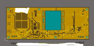
We are doing 300W isolated Synchronous Pushpull, 24vin, 32vout, 225khz. PCB screwed in bottom of Alu enclosure. FETs are surface mount. 4 layer PCB. No daughter boards.
The attached shows the layer 2. All of that copper pour (yellow) is the same net as chassis.
You can also see where the planar transformer goes (the blue bit). You can also see the 6 screwholes by which the PCB screws into the Alu enclosure.

There 6 Y caps…
2 Y caps connect input ground to chassis connected coppe
2 Y caps connect input power to chassis connected copper
2 Y caps connect output ground to chassis connected copper
There is an output common mode choke but no input common mode choke.

Question…..
1…Why has a whole PCB layer been devoted to chassis?…..it is directly over the bottom mounted FETs…..and so the FET switching nodes will be pumping common mode noise into the shown chassis copper pour. Do you agree this chassis copper pour should not be there?
 

Attachments

  • Chassis layer.jpg
    Chassis layer.jpg
    148.1 KB · Views: 112

Difficult to say but there doesn't look to be much clearance either. You'd need to look at the 0V layer with respect to CM Noise because if theres a return plane between the switching node and earth plane then CM Noise is likely reduced. Probably a question for the designer.
 
Probably a question for the designer.
Thanks, the guy who designed it gave us this design with a schem (for this layout) with a digital isolator (instead of an opto) which is placed so as to carry the secondary side error amplifier output across the isolation barrier!!!...so i am not sure about taking advice from him.

Also, well spotted for spotting that gap in the chassis layer , which looks like some type of isolation barrier...but , as you well imply, its only 0.375mm wide...and the isolation spec is 1500V.
Not only that, but the secondary bit is connected to the metal chassis, and the primary bit is connected to the same chassis, so i do not know what is going on there!
 
Last edited:

Thanks, the guy who designed it gave us this design with a schem (for this layout) with a digital isolator (instead of an opto) which is placed so as to carry the secondary side error amplifier output across the isolation barrier!!!...so i am not sure about taking advice from him.

Also, well spotted for spotting that gap in the chassis layer , which looks like some type of isolation barrier...but , as you well imply, its only 0.375mm wide...and the isolation spec is 1500V.
Not only that, but the secondary bit is connected to the metal chassis, and the primary bit is connected to the same chassis, so i do not know what is going on there!
I don't think the isolater will have much of job to do in this case. Could make a nice coaster :)
 
The following document...
...on pages 86-96, shows the chassis copper being used as a copperpour right under a SMPS Power module.
(several 100 Watts).
They give no rationale for this.
It appears to be madness, as the common mode noise from the switching stage will just get coupled into the chassis more easily, via this plane (the chassis plane is shown in tellow).....which is precisely what is not wanted.....all common mode noise filtration is designed around stopping noise capacitively and radiatively coupling to the chassis.
So do you know why they do it liek this?
The Vicor guide states its for EMI, its not madness as you don't have details of the module layout or what standard they're trying to comply too for this application note and they do say in the write up on Page 84 Section 1a that Y-capacitors (C15, C16, C18, C19) are there for CM reasons, they arn't on the circuit diagram though but they are on the board layout.
 
....yes i see your point.....in this case, the "chassis" that it refers to is the chassis of the power module, and not the chassis that will surround the whole thing (PCB and power module).
I see the Y caps that you refer to.....it does look like the reason for the chassis copper pour of page 87, is so that there's something to connect the y capacitors too, since they cant be soldered to the chassis of the DCM module itself.
No i believe chassis is chassis as your original assumption but the use of the capacitors provide a low impedance path for the CM noise to return back to source (i.e the DC/DC) locally thus the current going onto the exterior chassis will be limited and thus limit the CM Currents coming back up the power lines. I don't know the value of said Y caps but if a application has limitations on the size of them or a more agressive specification then there may be a need for a CM choke which is shown on page 37, Fig 2.39.
 
Thanks, i think your noticing the 4 y capacitors (C15, C16, C18, C19) on the diagram of page 87 of this...

...has clinched it. You can actually see how the chassis copper pour is soldered to the 4 corner pins of the module, and then the Y capacitor is right there in each corner,

It appears obvious that the chassis copper pour should have been 4 little pieces near these corners, and no more than that...ie, just enough to solder on the y capacitors.

The area of chassis copper pour that appears under the DCM module should not be there......it should instead be made of circuit ground........half primary ground, and half secondary ground.

"Chassis copper pour" in itself is the anethema of EMC good practice.....its disastrous...the entire premise of common mode EMC is "thou shalt not couple circuit "noise" into chassis".......so making a copper pour out of chassis is just inviting the switching nodes to couple capacitively to the chassis copper pour.

The diagram of page 87 shows a total violation of common mode EMC good practice.
 
Last edited:

Thanks, i think your noticing the 4 y capacitors (C15, C16, C18, C19) on the diagram of page 87 of this...

...has clinched it. You can actually see how the chassis copper pour is soldered to the 4 corner pins of the module, and then the Y capacitor is right there in each corner,

It appears obvious that the chassis copper pour should have been 4 little pieces near these corners, and no more than that...ie, just enough to solder on the y capacitors.

The area of chassis copper pour that appears under the DCM module should not be there......it should instead be made of circuit ground........half primary ground, and half secondary ground.

"Chassis copper pour" in itself is the anethema of EMC good practice.....its disastrous...the entire premise of common mode EMC is "thou shalt not couple circuit "noise" into chassis".......so making a copper pour out of chassis is just inviting the switching nodes to couple capacitively to the chassis copper pour.

The diagram of page 87 shows a total violation of common mode EMC good practice.
No, The ground plane under the DCM is meant to be there as it provides the capacitive path for the emissions to go into the copper and return to the DC/DC converter via the Y Capacitors which keeps the CM emission loop small. Remember, the current will go the path of least impedance BACK TO SOURCE so a low impedance capacitor will provide a path back to where it came from. If the capacitors are not there then the likelyhood is the noise would go the next best route which would likely be out of the chassis, through the ground plane of the test house, through the LISN and back up the power lines which would likely give conducted and radiated issues. It will still do this to some extent but thats why you have limits to comply too.
 
Last edited:
No, The ground plane under the DCM is meant to be there as it provides the capacitive path for the emissions to go into the copper and return to the DC/DC converter via the Y Capacitors which keeps the CM emission loop small.
......i dont disagree that what you are saying happens in the case shown......but why put up with it?.....why not make that chassis layer equal to the actual cct ground and let it couple into it directly?.....that's an even lower impedance path......And you can have the Y capacitors aswell......but just connecting to a bit of "chassis" copper at each corner of the module, (where the chassis pins are) and of course, to the Y caps.

...Its like you can drive London to Birmingham via Glasgow...........but its easier to just go up the M40 and go direct. I believe i have snowed the question and its leading to the analysis given, i do apologise for this. I believe you would agree with what ive just said, and would have already known it.

Coming back to it...
"Chassis copper pour" in itself is the anethema of EMC good practice.....its disastrous...the entire premise of common mode EMC is "thou shalt not couple circuit "noise" into chassis".......so making a copper pour out of chassis is just inviting the switching nodes to couple capacitively to the chassis copper pour.
I would say electrical safety is likely more important as the heat sink is connected to earth to prevent a shock hazard. Sandwitching the the module between earth on top and bottom will also be good for radiated emissions also and the Y capacitors provide the low impedance path for the CM currents. Like i said in my previous post its only a development board from what i can tell so makes very little claims in terms of compliance or specifications met, you'd have to evaluate it it and make your own judgements but looking at their design i wouldn't say it looks unreasonable given what it is and they provide a lot of documentation within that document as a guide to get to compliance such as using CM filters etc...
 
Last edited:
Sandwitching the the module between earth on top and bottom will also be good for radiated emissions
...but then you end up breaking the golden rule of common mode EMC stated with the bold text in post #12
 

...but then you end up breaking the golden rule of common mode EMC stated with the bold text in post #12

The way i see it is the RF is capacitvely coupled into the heatsink, and returns via 4 earth pads on the PCB through the Y caps back to the DC/DC so they arn't putting the current into the Chassis per se just the chassis node close to the DC/DC. I.e keeping the loop small
 
Last edited:
Thanks, and we agree 100% on what you have said there. The thing is, there is no need for that yellow chassis pour to be so big, and IMHO, it should not be.......it should just be a little bit (4 little bits) near the chassis pins of the DCM module....for connection of the SMD Y caps.
 

Thanks, and we agree 100% on what you have said there. The thing is, there is no need for that yellow chassis pour to be so big, and IMHO, it should not be.......it should just be a little bit (4 little bits) near the chassis pins of the DCM module....for connection of the SMD Y caps.
The Plane has 2 purposes,
1. Thermal
2. It forms the capacitive path for emissions
 
Status
Not open for further replies.

Similar threads

Part and Inventory Search

Welcome to EDABoard.com

Sponsor

Back
Top