Continue to Site

Welcome to EDAboard.com

Welcome to our site! EDAboard.com is an international Electronics Discussion Forum focused on EDA software, circuits, schematics, books, theory, papers, asic, pld, 8051, DSP, Network, RF, Analog Design, PCB, Service Manuals... and a whole lot more! To participate you need to register. Registration is free. Click here to register now.

[SOLVED] Triangular Wave generation

Status
Not open for further replies.

atancic

Newbie level 6
Joined
Jun 2, 2022
Messages
13
Helped
0
Reputation
0
Reaction score
0
Trophy points
1
Activity points
113
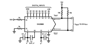
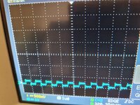
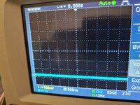
Hello, I am trying to generate different waveforms. I started with generating square wave. Once I managed to do it, I switched to triangular and this is my code below. I am using DAC800 and when I run the simulation it looks to me that the code is good as values of dac_out change as they should but when I implement it on the board I do not get the desired output on the oscilloscope.
Am I making a mistake somewhere in the code?


Code:
library IEEE;
use IEEE.STD_LOGIC_1164.ALL;
--use ieee.numeric_std_unsigned.all;

-- Uncomment the following library declaration if using
-- arithmetic functions with Signed or Unsigned values
use IEEE.NUMERIC_STD.ALL;

-- Uncomment the following library declaration if instantiating
-- any Xilinx primitives in this code.
--library UNISIM;
--use UNISIM.VComponents.all;

entity triangulartest1 is
    Port (clk, reset : in STD_LOGIC;
    dac_out : out STD_LOGIC_VECTOR(7 downto 0));
end triangulartest1;

architecture Behavioral of triangulartest1 is
signal flag : natural;
signal temp : unsigned(7 downto 0) := "00000000";
begin
process(clk)
begin
if temp = "00000000" then flag <=0;
end if;
if temp = "11111111" then flag<=1;
end if;
if (rising_edge(clk)) and (flag = 0) then temp<= temp + "00000101";
dac_out <= std_logic_vector(temp);

elsif (rising_edge(clk)) and (flag = 1) then temp<= temp - "00000101";
dac_out <= std_logic_vector(temp);

end if;
end process;

end Behavioral;
 

That’s right, you have to make sure that the LSB of dac_out gets mapped to the FPGA pin that’s connected to the DAC LSB pin, etc. The constraint file is half the story, the schematic (or PCB layout) is the other half.
Attached below is the schematic of the dac that I am using, and pins mapped (picture in my previous reply) are connected in order from lsb to msb. Even when I reverse the order, the output is similar, voltage is changed(0-0.5V in stead of 9.5-10V). I will try to simultaneously check on the scope each of the bits and the dac output as I have no clue why this is happening.
--- Updated ---

So far what I found out is that as I read pins starting from LSB to MSB, the output waveforms are getting more and more distorted in comparison to the LSB. It seems as if MSB does not go to 0 at any point for some reason. The board is new so I do not believe that something is faulty with the pins, I assume I do not know something about the board and that therefore this is the consequence. Are there particular pins that I should choose maybe?
 

Attachments

  • image_2022-06-04_172159606.png
    image_2022-06-04_172159606.png
    24.4 KB · Views: 115
  • lsb.jpeg
    lsb.jpeg
    208.6 KB · Views: 108
  • msb.jpeg
    msb.jpeg
    208.4 KB · Views: 110
Last edited:

Theres no reason to declare dac_out as buffer, it’s an out.

Also no reason to use case statement, a nested if-then-else will suffice.
Why not? What does buffer mean here?
dac_out : buffer std_logic_vector(7 downto 0);
Also, what's wrong with using case statement here?

atancic, what simulator are you using? I probably would ask that you show your simulation here.
--- Updated ---

Attached below is the schematic of the dac that I am using, and pins mapped (picture in my previous reply) are connected in order from lsb to msb. Even when I reverse the order, the output is similar, voltage is changed(0-0.5V in stead of 9.5-10V). I will try to simultaneously check on the scope each of the bits and the dac output as I have no clue why this is happening.
--- Updated ---

So far what I found out is that as I read pins starting from LSB to MSB, the output waveforms are getting more and more distorted in comparison to the LSB. It seems as if MSB does not go to 0 at any point for some reason. The board is new so I do not believe that something is faulty with the pins, I assume I do not know something about the board and that therefore this is the consequence. Are there particular pins that I should choose maybe?
Why are you gating the clock? Do not AND the clock with another signal.

Also, I believe the timing here isn't as expected either. It would be way shorter than expected if your counting starts off in the wrong direction. Confirm that the period of the waveform is correct. Your initialization or count can make your signal start off in the wrong direction. Let's start from here. Initialize flag to 0. With your step size of 5 Set flag to 0 at temp=5 and set it to 1 at temp=250 (I'd prefer to use NOT flag repeatedly rather than explicitly use 0 and 1). Realize that this will cause temp to increase to 255 (i.e. one clock cycle later) before beginning to decrease. And it will cause it to decrease to 0 (i.e. one clock cycle later) before increasing again.

I repeat: you can declare dac_out as buffer. There's no problem with that. You can use case statement with if statements embedded within it or you can use pure if-else statements. The choice is yours.
--- Updated ---

Sorry can you please tell me if I understood "pin mapping" term correctly? I googled about the meaning but so far I did not find any explanation. I thought that bit mapping is dedicating outputs from the code to the on-board pins, LEDs, 7 segment etc. Am I correct or I completely misunderstood? Picture for a reference of how I declared the pins on the board in MIMASV2.ufc .
Also, note that dac_out(7) has to be connected to B1 of DAC0800, dac_out(6) to B2, dac_out(5) to B3, ..., dac_out(0) to B8.
 
Last edited:

as akanimo points out, B8 on the DAC is the LSB. ( Why the mfr would do that is beyond me).

But i’ll bet anything you’ve got it backwards.

As far as using case vs if-then, maybe it’s just a personal preference, but case statements are used when the control variable can have multiple values, in the OP’s case it’s a single bit. You’ll write more lines using a case statement, i think.

And as far as using buffer instead of out, it’s not “wrong” but certain tools may have trouble, especially if you don’t have ALL the higher level modules also using buffer. In my years and years of writing VHDL i’ve never used buffer.
 

    atancic

    Points: 2
    Helpful Answer Positive Rating
Yes, there is potential for conflict if the higher level modules are not also using buffer mode and with tool-specific implementation. So be wary of this. I have used the buffer without having trouble.

The case statement may increase the lines by a little bit, in this case, maybe by one or two. However, it should be expected that to improve resource utilisation.

barry, it seems like the one-cycle delay is causing the counter to go something like: 255 -> 0(256) -> 255 -> 250 -> 255 -> 0(256) -> and so on.
 

    atancic

    Points: 2
    Helpful Answer Positive Rating
Why not? What does buffer mean here?
dac_out : buffer std_logic_vector(7 downto 0);
Also, what's wrong with using case statement here?

atancic, what simulator are you using? I probably would ask that you show your simulation here.
--- Updated ---


Why are you gating the clock? Do not AND the clock with another signal.

Also, I believe the timing here isn't as expected either. It would be way shorter than expected if your counting starts off in the wrong direction. Confirm that the period of the waveform is correct. Your initialization or count can make your signal start off in the wrong direction. Let's start from here. Initialize flag to 0. With your step size of 5 Set flag to 0 at temp=5 and set it to 1 at temp=250 (I'd prefer to use NOT flag repeatedly rather than explicitly use 0 and 1). Realize that this will cause temp to increase to 255 (i.e. one clock cycle later) before beginning to decrease. And it will cause it to decrease to 0 (i.e. one clock cycle later) before increasing again.

I repeat: you can declare dac_out as buffer. There's no problem with that. You can use case statement with if statements embedded within it or you can use pure if-else statements. The choice is yours.
--- Updated ---


Also, note that dac_out(7) has to be connected to B1 of DAC0800, dac_out(6) to B2, dac_out(5) to B3, ..., dac_out(0) to B8.
As for the simulation, I am using XISE for coding and simulation.
My code has changed since then and I no longer have clock ANDing with other signals. I will post it below to avoid any confusion.
Code:
process(clock)
begin
if temp = "00000000" then flag <='0';
elsif temp = "11111111" then flag <='1';
end if;
if rising_edge(clock) then
if flag = '0' then temp <= temp + "0000101";
elsif flag ='1' then temp <= temp - "00000101";
end if;
end if;
dac_out <= temp;
end process;
Temp is initialised as "00000000" and therefore for the first 'if' line will always set flag to 0, which will therefore lead to incrementing. As for the LSB and MSB, I tried inverting and reverting them to see if something will drastically change, however just the voltage level changes and the output is still 0.5V difference from top to bottom of the wave, where it should have been ~10V difference. It seems as if the latter bits/pins (no matter the order, whether the pin mapping is correct or inversed) do not switch between "on" and "off" states but just stay "on" all the time, as per my oscilloscope reading. To make it more clear, if I inverse the pin mapping, different pins will be "stuck" at "1" when compared to the correct pin mapping, but the issue still persists, pins are not changing logic level when they should.
 

@atancic you’re just not paying attention.

You STILL have 253 undefined conditions for temp in your if statement.

Why do you assign flag outside of the clock statement, but you assign temp inside the clock statement?
Further, you don’t have temp in your sensitivity list, so your simulation will probably be wrong.
Don‘t put your assignment on the same line as your “then”.
Indent your code so it’s easier to read.

Just “inverting” the pin mapping (I presume you mean reversing) doesn’t prove anything. Have you verified that all 8 FPGA pins go to all 8 DAC pins? Have you looked at those DAC pins with a scope, as suggested?
And i would suggest you have everything clocked.
 

    atancic

    Points: 2
    Helpful Answer Positive Rating
You have not synchronized the counter with clock. In your process, you have to enclose everything within the if statement of the clock. barry has also pointed that out, so correct it.

You have to realize that at flag is set to 1 in the next clock cycle after temp=0. By then temp is either 5 or -5 depending on the initial count direction. Explicitly initialize flag to 0. Do not use 0 and 255 to set and reset flag. Use 5 and 250 instead. Cut line 3 of your code snippet in post #25 and insert it inbetween line 7 and line 8 and then end that if statement. Your line 4 (which would be if instead of elsif) should be immediately after the elsif for flag and you end that if statement.

I believe that if you make these corrections, you would have an output from the DAC0800 that would ramp up and down from -10V to 10V.
 
Last edited:

    atancic

    Points: 2
    Helpful Answer Positive Rating
If it be the case that you have 10V and -10V as peaks of the triangle waveform from DAC0800 (assuming you have a Vref of 10V), then you should just need to change the value 5 in the 5 and 250 combination to a value 5 above halfway of 256. But then a step size of 5 would not be a good value for a quick design testing, so you'd have to change to the appropriate step size of 1 and a 1 and 254 combination in place of the 5 and 250 combination. The combination would now be changed to 129 and 254 to get the triangle wave to be at about 0V to about 10V peaks.

Anyways, when you have made the corrections, post your corrected code let's be sure you understood what corrections you were asked to make, and also post the DAC0800 scope waveform let's see the result. From there, we may have to look at the DAC0800 circuit.
Actually your first reply worked. I swapped the code lines as you suggested and changed the flag triggering limits to "00000101" and "11111010" (5 and 250) and the output is a nice triangular waveform. I also tried incrementing by 1 instead of 5 but the output is nicer when it is incrementing/decrementing by 5 so I .left it as it is. Thank you both @barry and @Akanimo !
 

Status
Not open for further replies.

Part and Inventory Search

Welcome to EDABoard.com

Sponsor

Back
Top