Continue to Site

Welcome to EDAboard.com

Welcome to our site! EDAboard.com is an international Electronics Discussion Forum focused on EDA software, circuits, schematics, books, theory, papers, asic, pld, 8051, DSP, Network, RF, Analog Design, PCB, Service Manuals... and a whole lot more! To participate you need to register. Registration is free. Click here to register now.

High Voltage output SMPS shouldnt use basic TL431/Opto feedback?

Status
Not open for further replies.

cupoftea

Advanced Member level 5
Joined
Jun 13, 2021
Messages
2,584
Helped
54
Reputation
108
Reaction score
115
Trophy points
63
Activity points
13,565
Hi,
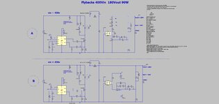
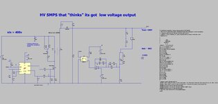
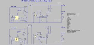
When we do SMPS with high voltage output, like 180Vdc, then its more difficult to avoid ending up with a very unfortunately low feedback loop bandwidth….
Therefore, for eg an opto-isolated SMPS as attached, its very important to do the feedback loop like in Circuit “B” of the attached. Circuit “A” has two paths from Vout to the error amplifier, and these paths 'fight' against each other……and in solving this you end up with an unfortunately lower feedback loop bandwidth.

(LTspice simulation and jpeg schem as attached, shoudl you wish)

So do you agree, Circuit “B” is better?

(Also attached is the LTspice Sym and Sub files for the TL431...should you wish for them)
 

Attachments

  • Flybacks 180Vout.jpg
    Flybacks 180Vout.jpg
    169.5 KB · Views: 298
  • LTspice _TL431 MODEL FROM HELMUT.zip
    1.2 KB · Views: 138
  • Flyback 400V TO 180V 0A5 out.zip
    4.3 KB · Views: 137

Far better to have a 15V say aux supply for the secondary, then dividers for the Vout ( with compensating caps if required ) then a decent op-amp driving the opto LED ( which LED should be for e.g. an HCPL4053 - which has an internal CM screen - and is fast and low gain - all good things ) and a good design for allowing for the opto xtor to control the pwm.

If you are truely seeking good bandwidth - this is the way to go.
 
Hi,
The HCPL4503 as you say is a fast optocoupler. We wish to use it to control our isolated 2kW LLC converter which has Vout=180Vdc. (Vin=400Vdc).

The LLC controller is ICE2HS01G...

ICE2HS01G
https://www.infineon.com/dgdl/Infin...n.pdf?fileId=db3a30432a40a650012a458289712b4c

The opto collector must draw between 39uA to 323uA from the ICE2H’s FREQ pin in order to regulate the LLC converter (ie change the switching frequency). The FREQ pin is regulated to 2V. The ICE2H detects the current pulled from the FREQ pin, and adjust s f(sw) accordingly.

The problem is that the HCPL4503 datasheet only gives CTR for opto_diode currents from 5mA upwards. 5mA in the opto_diode would mean 5 x 0.3 = 1.5mA being drawn by the opto_collector…..this is way too much for ICE2H…

Must we assume that we cannot use the HCPL4503 for our case?

Or perhaps we can if we do the attached?

HCPL4503
 

Geez Wayne, the opto coupler will work like any other, obviously 39uA to 323uA is a point of noise entry to the control IC - but apart from that there is no reason why the 4503 will not work just fine.
--- Updated ---

... the lower CTR at lower LED currents is actually beneficial here ( in case you missed that salient point ).
 
While low-current CTR is more susceptible to aging perhaps,
it is something you could characterize across batch and
accelerated lifetest* without much effort.

* if you had an idea of what accelerates LED / opto insulator /
photodiode / gain transistor degradation, to what factor,
offhand....

The datasheet CTR description appears to put the output
BJT in soft saturation, and is not the CTR you'd see at the
feedback pivot point or a logic threshold (unless you're using
0.9V logic). The test condition puts you somewhere on the knee
(or ankle...) of CTR vs VOL.

If you want a controlled CTR / current across variables then
recommend you use one of those feedback optos (i.e. a
single emitter with two transistors, one for local feedback
on the secondary side error amp and one for "real" feedback
to the primary side controller) and hope matching holds up.
 
Hi,

optocoupler CTR degradation:
I used optocouplers (high quality brand) rather at the lower end of "typical operation current", pulsed (not continously ON) in an industrial application, (ambient temperature never above 30°C). They failed within 5 years by dropping their CTR below 30% of the initial value. I luckily had the optocouplers from same batch (datecode) in stock to compare with.

I did not expect this. From this time on I drove them with higher current. and also tried to avoid optocuplers.

I mean for a small company, specialized to design low volume special industrial equippment .. there is no chance to do "long term tests" beforehand.

Klaus
 
Thanks, i must admit it surprises me hearing about fast opto's, since so many vendors are touting alternative ways to optos, eg "Digital isolator FET drive from sec side", so that feedback opto's can be avoided, precisely because of their proclaimed slowness...but now here's one thats quite fast.

Also, we anticipate control problems due to the high voltage output of our 180Vout (390Vin) , 2kW LLC. ...And just wondered whether the attached method of "making a high voltage output look like a low voltage output" has any mileage?
...It uses a divider and emitter follower to make the 180Vdc "look like" 30Vdc.
Is this of any use?
(LTspice sim, LTspice .sym and jpeg schem attached should you wish)
 

Attachments

  • High voltage SMPS that thinks its low voltage.jpg
    High voltage SMPS that thinks its low voltage.jpg
    172.3 KB · Views: 203
  • Flyback 400V TO 180V 0A5 out_HV trick.zip
    2.9 KB · Views: 99
  • LTspice _TL431 MODEL FROM HELMUT.zip
    1.2 KB · Views: 100

Also, do you think the attached is OK for implementation of the fast HCPL4503 opto?.......it has a Vcc pin...something i have never seen in any SMPS schematic, and not seen in any of the offline SMPS's i have taken apart. I allowed for up to 5mA of opto_diode current, just to be sure i can get the 323uA maximum current in the opto_transistor.
 

Attachments

  • opto.pdf
    114.3 KB · Views: 129

As you know, error amplifiers etc are down at ~5vdc.....but 180vdc otuput is well above that...so it needs to be divided down before the controller can operate on it...and thats where the problem starts in the control loop. The controller "sees" the output through the divider...and since the divider decimates the heck out of it when vout is high..the controller then struggles a little.
I used to work in a HV SMPS place many years ago, and i remeber them saying they were only going to achieve loop bandwidths in the Hz range for some of their HV supplies.

Also, i think the added capacitor (as attached) improves things.....it needs the cap, otherwise its just another way of dividing down............at first glance, the one with the cap looks great in terms of transient response etc...and lack of overshoot on startup.

LTspice and jpeg schem attached
 

Attachments

  • High voltage SMPS that thinks its low voltage_with capacitor.jpg
    High voltage SMPS that thinks its low voltage_with capacitor.jpg
    177 KB · Views: 191
  • Flyback 400V TO 180V 0A5 out_HV trick_with capacitor.zip
    5 KB · Views: 113

Hi,

Embarrassingly stupid question to hang my head in shame about: What's the base voltage of Q4 (Q2)? Calculator says 180V x (2k/12k) = 30V; datasheet for 2N5550 says (unsurprisingly) 6V is maximum Vbe... I can understand that it's related to the 30k to ground on the emitter of Q4 (Q2) - does that create a 'false ground' for the BJT so Vbe never rises above the Vout ripple voltage or something along those lines and Vbe is never over a volt or so? What's the expected voltage at Q4 emitter and how is it calculated? Or put differently: How is Q4 (Q2) biased? - I assume Q4 Ve is 180V - Vce, and IC is ~ 6mA. I understand the premise to be Vbe = ~ (Ve + Vbe), not how it's achieved. Thanks.
 
Thanks.... as i believe you have gathered, the whole idea of this is to make the 180V output "Look like" a 30V output to the controller. Hence the divider to divide the 180V down to 30V.....then this is fed to the emitter follower with Q2.....yes you just look at emitter of Q2 being 0.7V below its base voltage all the time.

The idea i believe is a fantastic way of regulating high voltage SMPS.

I couldnt just divide down the 180v and then feed that to the "controller's divider"...as it would have been too high impedance....so i put the Q2 there....so the "30v divider" sees the output through the emitter of the Q2, which looks like a low impedance........because when you "look" into the emitter of a common collector BJT (Q2), you are "seeing" into a low impedance.....Anyway, what i actually wanted to do, was to transport any ripple/fluctuation voltage on the 180v rail directly down to the "30v rail"...without it being divided down....so that it really does look like a 30v rail.........i wanted to kind of copy/paste the ripple of the 180v rail to the "30v rail"....so i put also the capacitor across the base resistor of Q2....so that at high frequency, i am literally shorting the 180v ripple to the "30v rail" (or trying to)..and the controller will then be fooled into believeing that it really is regulating 30v.

The intial results look very promising......when we try to regulate high voltage...we have to divide it down heavily...and this messes things up for the controller...because it then has to have gain added to overcome the high attenuation of the divider, and thats when problems start...because the gain will act on many things.......not just the thing we want it to....this is why HV SMPS have more limited options for feedback loop regulation.....eg start up vout overshoot is much harder to solve with HV outputs...not only that.....but when you dont do it like the above...then your compensation capacitors across the upper divider resistor have to be 250V rated caps...which is a pain when you need to tweak them........why not just take it all down to 30V, and then work on it there with your standard 50v ceramic compensation caps.?......i honestly believe the above is the untold secret of high voltage SMPS feedback regulation....the only problem might be sourcing high enough voltage NPN's for Q2.......though a Darlingtom would work there.
--- Updated ---

It is absolutely doubtless that HV SMPS's present more difficulty for SMPS feedback loop regulation.......i used to sit near one of the best HV SMPS designers in UK....he was a top guy at the Marconi place...i overheard him and the softy talking about how they would regulate their new HV SMPS (>13000v output).....they were discussing that they would only be able to manage a feedback loop bandwidth in the "Hz range". (they werent talking about the PFC bit)
 
Last edited:

    d123

    Points: 2
    Helpful Answer Positive Rating
...As you know, the fact you have a 200:1 divider in the overall loop, means you then have to bring in extra gain to take account of that...but bringing gain into a feedback loop is not simple to do...that extra gain will mess things up in other ways .....making the feedback loop options more limited.
As you know, when you have a 200:1 divider, compensating it is not as simple as just putting in an amplifier, with sufficient gain to take account of the 200:1 attenuation........its just not that simple.........for that degree of attenuation, finding how to put the gain back into the loop is very complex, and always restrictive in terms of possible outcomes....this is why HV SMPS are so non-conducive to good feedback loop compensation.
 

the divider - as long as it is linear with frequency - has no effect on the feedback loop whatever - it simply matches Vout to something the error opamp can handle.
--- Updated ---

the main reason VHVDC power supplies have slow loops is that:-

1) overshoots need to be avoided - hence heavily damped control loops

2) the capacitance associated with the step up Tx makes the power stage slow - hence the control loop must be slower.

3) voltage multipliers and similar have very slow responses to load change - hence slow & damped control needed.
 
  • Like
Reactions: cupoftea

    cupoftea

    Points: 2
    Helpful Answer Positive Rating

    d123

    Points: 2
    Helpful Answer Positive Rating
1) overshoots need to be avoided - hence heavily damped control loops
Thanks, it seems that the attached emitter_follower_with_cap method makes it easy to compensate to avoid overshoot....noticed when running the LTspice simulation.
Also, it does mean when tweaking the feedback cap across the upper divider resistor.....low voltage (50v) caps can be used....this in itself seems very good, and cheaper.

If nothing else, the emitter followed method does seem to make compensation easier?......just from playing with it in LTspice
 

the emitter follower - as you call it - simply puts all the heat - that would otherwise be in resistors into a bjt - is this what you really want to do ?
 
Status
Not open for further replies.

Similar threads

Part and Inventory Search

Welcome to EDABoard.com

Sponsor

Back
Top