Continue to Site

Welcome to EDAboard.com

Welcome to our site! EDAboard.com is an international Electronics Discussion Forum focused on EDA software, circuits, schematics, books, theory, papers, asic, pld, 8051, DSP, Network, RF, Analog Design, PCB, Service Manuals... and a whole lot more! To participate you need to register. Registration is free. Click here to register now.

Reducing high-frequency noise in Active PFC

Status
Not open for further replies.

mike buba

Member level 2
Joined
Nov 17, 2013
Messages
50
Helped
0
Reputation
0
Reaction score
1
Trophy points
1,286
Activity points
1,707
Hi all,

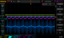
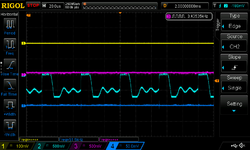
I am building an Active PFC circuit (Vin = 230 Vac, Vout = 700 Vdc, Pout = 4 kW) and I am noticing noise when the switch Q1 on the figure is on. One can assume the noise is visible on the oscilloscope because of the Ch4 current clamp poor filtering since I am also using another clamp to measure a DC current (Ch3) and there is no noise. Ch4 (blue) is input grid current, Ch3 (purple) is inductor L1 current. There is also an EMC filter Shaffner FN2030-30-08 at the input.
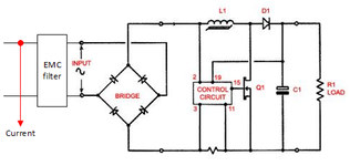
Drawing1.png
But when I compare two similar cases (same input voltage and power) with Q1 turned off and on, the noise is there, so the Ch4 probe, because of low filtering, just amplifies it.
Switch Q1 turned off
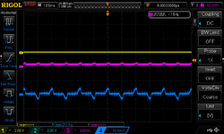
DS1Z_QuickPrint33.png
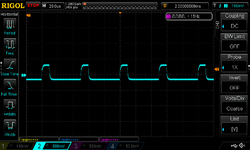
Switch Q1 turned on
DS1Z_QuickPrint34.png(Vout = 60 Vdc, Iout = 0.2 Adc)
Switch Q1 turned on
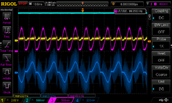
DS1Z_QuickPrint42.png(Vout = 350Vdc, Iout = 1.7 Adc)
I measure 6.6 kHz and 34.8 kHz spikes. Q1 switching frequency is 20 kHz.
I was trying hovering the current probe at the same distance from the converter above the components to try to see if there is a place with the 'bigger' noise, but I cannot see the change in the amplitude or intensity.

Are there any ways to reduce the overall noise in the converter?
I suspect the increased amount of noise is later affecting serial communication which breaks down at higher powers and voltages.
 
Last edited:
The "fuzzy" noise that you see.....as you say, its still there even when the FET is not switching, but not quite as much........is just common mode noise getting coupled into your scope probe from the surroundings, including from your PFC.......there'll be SMPS's operating presumbaly all around you (eg lighting etc), so their noise is going to be coupling into your scope probe.

But you real prob is the serial comms breakign down at higher P and V.

So...to make a PFC less noisy.

BTW is it a boundary mode pfc?...if so, these are good for getting rid of reverse recovery noise....you need a specific Boundary mode controller, which "waits" till your inductor has discharged fully before turnign the fet back on.

Whats your max power level.?...because boundary mode is better for the lower powers , otherwise the peak currents can get very high....but boundary mode (aka critical mode pfc) is very good at reducing noise of boost pfc's.

I woudl use SiC diodes and FETs, (if you are doing continuous mode pfc) since you have vout = 700v....this woudl reduce noise from reverse recovery of the output diode.
Also, you can slow down the turn on of your fet in order to reduce noise.....do this by eg putting a capacitor from gate to source, or increase the series gste resistor.
...dont do this too much otherwise your fet will overheat.
You can also add tight capacitive decoupling close in to your power switch loop, and the rectifier loop.

And of course...tight PCB layout....the attached tells the tricks of this.

Also, some common mode filtering at the input woudlnt hurt...but you say you already have a filter module?

Other thann that, there is of course, shielding with metal. You coudl also add an output diode RC snubber.

Also, what kind of serial comms is it......what speed?....as you know, you can roll your own serial comms protocol to make it more noise immune...eg make it very slow, and sample the ones and zeros multiple times so you dont detect it wrong etc etc.....also, things like shielded cables, and twisted pair etc.
 

Attachments

  • Basics of SMPS Layout _4.zip
    543.1 KB · Views: 155
Last edited:

    mike buba

    Points: 2
    Helpful Answer Positive Rating
" Are there any ways to reduce the overall noise in the converter? "

Yes there are, slowing turn on of mosfet, using SiC diode, thick Al2O3 washers and thermal grease to heatsink for the semi's, reducing switching loop area to absolute minimum in the layout, quality film / foil decoupling caps close to the mosfet and diode, shielding of the boost choke, making sure the sw node goes to the inner wdg part of the boost choke, heatsinks tied to 0v the list goes on ...
 

thick Al2O3 washers and thermal grease to heatsink for the semi's

Thanks for this one, please could you possibly elaborate?....maybe OP also would need the elaboration for this one?
 

Other thann that, there is of course, shielding with metal. You coudl also add an output diode RC snubber.
It is 3 kW max output power. I am seeing noise at even low powers, for example, Vout = 200 V and Iout = 1A.
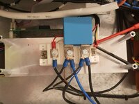
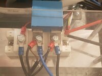
I am using the Semikron SKM100GAL12T4 IGBT module and driver SKHI 10_12 (R) (I know, overkill for the application, 10x higher max. current, but there were some changes to the initial 'compact' design). The heatsink is grounded, the inductor is shielded, there is a snubber capacitor across IGBT (1uF, 1kV).
The switching frequency is 20kHz.
Power cables are not shielded, but all signal cables are shielded and grounded on one side.

20220213_002532.jpg

I was thinking of adding a resistor in series with a snubber capacitor as I have read this drastically reduces ringing, while the capacitor primarily reduces the frequency. Some suggest for resistor do V / I 700 / 5 = 140 Ohm, while this gives 1.7 kOhm (Ipeak = 5 A, Vrail = 700 V, rise time = 0.2 us (ton from IGBT datasheet) and 20kHz)?!
 

The paper is discussing snubber capacitor parallel to switch transistor, your snubber is a DC snubber across IGBT pins 2/3, in parallel to C1, isn't it?
 

The paper is discussing snubber capacitor parallel to switch transistor, your snubber is a DC snubber across IGBT pins 2/3, in parallel to C1, isn't it?
Hm. Yes it seems 😕
So should I move that to 1 and 2 (across Q1) or keep that parallel to C1 and add another one across Q1?
 

Is this what you are using?


...are you using the other diode as the boost pfc diode?
Are you in CCM?

If so, you must use a SiC diode, or a few in parallel, or at least a ultra fast diode(s) with very low trr.......your main problem is likely to be severe reverse recovery of your boost pfc diode.

Can you answer these questions?...
1....Are you in boundary conduction mode (aka critical conduction mode)?
2....or Are you always in DCM?
3....or Are you in CCM?
4...What is the reverse recovery time (trr) of you boost diode?
5...Or are you using a SiC boost diode?

If you dont know the answers to all the above...then you need to find out these out first.....come back if you dont find on www, and i will give you some articles on the above.

BTW, you can sometimes get away without SiC diodes if you fsw is low, and maybe you use ferrtie bead in the collector of the IGBT, and you increase the switch on transition of the IGBT.

I must admit, i dont recomend IGBT for PFC FET...because of the tail time.

Use FET...and use parallel, alternate PFC stages if you need to...ie one does 10ms, then the other does 10ms etc etc
 

Can you answer these questions?...
1....Are you in boundary conduction mode (aka critical conduction mode)?
2....or Are you always in DCM?
3....or Are you in CCM?
4...What is the reverse recovery time (trr) of you boost diode?
5...Or are you using a SiC boost diode?
Yes. I am using SKM100GAL12T4. Starting topology was rectifier and DC/DC boost converter with an inductor at AC side, but now I converted to Active PFC (no input inductor).

1. It seems I am in the continuous mode if I look at the inductor current from my first post (Ch3).
2. No
3. It doesn't look like it. Inductor current never falls to zero during half-period, albeit I have not tried higher powers and voltages (max was 550 Vdc and 2.5 Adc).
4. I am using a chopper diode as D1. In the SKM100GAL12T4 datasheet I found tr (at Tj = 150 °C) = 47 ns. But I think this is for IGBT, nothing for Inverse diode or Freewheeling diode.
5. No. But I can bypass the chopper diode D1 with a Schottky or SiC diode. I will also replace the bridge rectifier from Fast recovery (trr 170 ns) to Soft recovery (trr 63 ns) and see if this helps.

I'll try ferrite beads. The PFC was not the initial design concept, and I am re-using components from the older solution.... so getting a SiC MOSFET is something I would like to avoid. Especially since I already have a bespoke control and interface board to Semikron driver.
 

If you use an RC snubber across a switching transistor, then if the R is too small. then it will not sufficiently curtail the sudden spike of current drawn out of the C when the FET turns on.....but you can simply increase the resistor until the spike is well damped.....then there wont be much noise......but on the other hand, the R should be low value enough so that when the FET switches off, the fet current can mostly divert into the snubber cap (and this in turn lowers the dv/dt at switch off) ...so its a bit of a compromise...basically you are looking to reduce the dv/dt and di/dt at the switching node(s).

Make sure your snubber loops are tight...(small in area)...as you know, its a general rule of SMPS that current loops shoudl be as small area as possible.

Have you grounded your heatsinks to earth ground?.....this is do-able, but will give more common mode noise than if you connect your heatsinks to local ground.

Also, i take it that you dont need isolation for your output?

Also, do you post your layout?...layout is massively important for noise reduction.
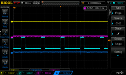
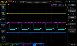
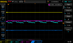
I recorded voltage across the IGBT in the chopper module (PWM set to 20%, Vout = 30 Vdc) as it is now and it seems the voltage is oscillating.

I can see four different cases. I hoped I would see either oscillation or not, but not sure why are there other three cases. Please see oscillograms and video. Please ignore other channels. Voltage accros IGBT (1 and 2) is Ch2

I am not sure if this is because of the no snubber or something else in the circuit?

DS1Z_QuickPrint49.png DS1Z_QuickPrint50.pngDS1Z_QuickPrint51.png DS1Z_QuickPrint52.png
Video:

PWM pulses
DS1Z_QuickPrint53.png

Would RC snubber help there, and if so how to design one? At the moment I have a capacitor across 2 and 3.

The heatsink is grounded, i.e. mounted to the cabinet base. This is how it looks. The DC(-) is not grounded as this is only the 1st stage (DC-bus for three-phase inverter).

20220220_170445.jpg
 

Status
Not open for further replies.

Part and Inventory Search

Welcome to EDABoard.com

Sponsor

Back
Top