Continue to Site

Welcome to EDAboard.com

Welcome to our site! EDAboard.com is an international Electronics Discussion Forum focused on EDA software, circuits, schematics, books, theory, papers, asic, pld, 8051, DSP, Network, RF, Analog Design, PCB, Service Manuals... and a whole lot more! To participate you need to register. Registration is free. Click here to register now.

[SOLVED] wide swing cascade current mirror design the ratio of w/l

Status
Not open for further replies.

r.mirtaji

Junior Member level 3
Joined
Feb 9, 2020
Messages
27
Helped
0
Reputation
0
Reaction score
0
Trophy points
1
Activity points
403
Dear friends,
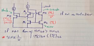
The following figure is the wide swing cascade current mirror
Why in design the ratio of \[ (W/L)3,4 \]is usually considered smaller than the ratio of \[ (W/L)1,2 \]

we know that \[ VoV↓ ∝ (L↓)/(W↑) ↓ \]

then Vov3,4 > Vov1,2 for example Vov1,2= .14v and Vov3,4=. 2v

Why don’t designer set the value of Vov equal for all transistors in the design?
 

Attachments

  • 2.jpg
    2.jpg
    381.8 KB · Views: 1,362

Cascode and mirror devices don't have to have the same size.
Fix the Vov of the mirror device, say 200mV or 150mV and plan to have maybe 20-30mV on top of it for the Vds of the mirror transistor. From that Vov and the current you can find W and L. Usually for small current like 5uA the size of the mirror transistor comes small. In this case perhaps mismatch is a better criterion of sizing it, that is you increase the W and maybe also L until you get the required matching. This can push you into weak inversion but if it does, so be it. Use large L for that transistor.
Cascode device can have minimum L or about there. Based on the minimum compliance voltage across your current source and the chosen Vov for the mirror device, you can choose the Vov of the cascode device and size it. Then you choose the voltage at the gate of the cascode device to be such that it results in the wanted Vds of the mirror device. Then you generate that gate voltage with transistors.
 

    r.mirtaji

    Points: 2
    Helpful Answer Positive Rating
Dear sutapanaki
So as I understood because of the mismatch between two transisitor
We usually consider the channel length of mirror Transistors to be 5 times of the minimum channel length.
And on the other hand increase of channel length Cause increase of Vgs And the transistor enters the sub-threshold area later
And for the cascade transistor according to the minimum voltage that the current source must operate in the saturation region
and Vov of mirror we can choose size of cascade Transistors
 

Yes, to decrease the mismatch in the currents, yo need more L. More L is actually making it harder for the transistor to go into weak inversion. Increasing W for fixed L makes it easier to approach weak inversion.
 

    r.mirtaji

    Points: 2
    Helpful Answer Positive Rating
Status
Not open for further replies.

Part and Inventory Search

Welcome to EDABoard.com

Sponsor

Back
Top