Welcome to our site! EDAboard.com is an international Electronics Discussion Forum focused on EDA software, circuits, schematics, books, theory, papers, asic, pld, 8051, DSP, Network, RF, Analog Design, PCB, Service Manuals... and a whole lot more! To participate you need to register. Registration is free. Click here to register now.
Hi,
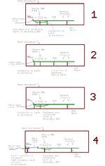
Which of the attached (1 to 4) is the best way to Earth the secondary of a PCB which is powered by an offline SMPS? (ie to reduce EMC problems)
The PCB is in a metal enclosure.
The option 4 is often seen; an Earth connection available on the chassis close to the power entry, as a bare screw. I would bet as being most appropriate, since any electrical discharge on the metal enclosure at the opposite side would not necessarily carry current through the PCB toward the power cable.
Thanks, and are you also saying that having the Earth connection at the mains power cable entry point gives reduced EMC emissions? (better chance of passing EMC test).
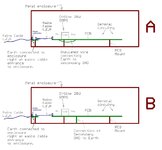
Also, if we agree that Earthing at cable entry point is best, then which is the best way to earth the secondary in conjunction with that...A or B in the attached?
I was rather referring to the expected reduction in the susceptibility of the electronic board inside to suffer malfunctions by suggesting the option 4 in post #1. In other hand, I presume that, from the point of view of electromagnetic emission, having the board as the aggressor, the differences of settings 1 to 4 in post #1 are somehow negligible, the metalic shield should do most the job.
Thanks for this, its the crux of it...the thing is, the "loop" through the wire and through the y cap across the isol barrier (transformer pri to sec) in 4 is a lesser area loop than the corresponding loop in 2...so it should be better regards EMC?
That’s what the wire is for…its to reduce the Earth loop area...and thence to reduce common mode emissions.
#4 might perform better, especially if proper feedthrough capacitors are used. Feedthroughs should help with any of the four configurations.
By a “feedthrough capacitor” in this case, I presume you mean like a diff mode (X2) capacitor, which has an earth connection to its case? -So that it kind of acts like an X2 capacitor and a very good Y capacitor?
This site uses cookies to help personalise content, tailor your experience and to keep you logged in if you register.
By continuing to use this site, you are consenting to our use of cookies.